
LED Ring Light Source - led light ring
Functional test is the last step of the inspection and verification process. As the name implies, its task is to test the functioning of a circuit, reproducing the electrical signals capable of stimulating it and measuring the effects produced. The circuit is correctly powered and electrically stimulated through the interface connectors. A software application processes the measurements performed at suitable points on the PCB, verifying their correspondence with the design specifications. The advantage of the functional test is its ability to detect potential circuit anomalies that occur only when the circuit is powered; moreover, it is also able to measure the power absorption in specific points of the circuit. The disadvantages are related to the cost and complexity of the test system. In fact, it requires very sophisticated, but not much flexible, equipment, most of the time configured to perform only the test of a specific card.
PCBboard inspection
180 degrees visibility, up to 500 meters. 6 high-intensity red LEDs. Integrated light sensor. Night-safe, steady or three blinking modes.
Boundary-scan is a technique introduced to test the interconnections between the components on the board and is widely used to test ICs when it is not possible to reach all the nodes of the circuit. The physical probes are replaced by "cells", whose output (TDO) and input (TDI) data pins are connected in sequence to suitable shift registers and to a circuitry for multiplexing. The boundary scan logic is timed by a TCK (Test Clock) signal, while a TMS (Test Mode Select) signal enables the test. It is thus possible to access the I/Os without having to place physical test points on the board, through a simple 4-wire serial interface (which becomes 5 if an optional reset signal is included) called TAP (Test Access Port). The Boundary Scan Description Language (BSDL) files, provided by manufacturers, contain information on boundary-scan components. The boundary scan method has the advantage of being suitable for several applications, including system-level test, RAM and flash memory test and CPU emulation. In addition, the test can be conducted directly on the field. On the other hand, its main disadvantage is that it is not an exhaustive test, the coverage of which is limited to the components which support this type of interface.
We offer the Best Outdoor LED Spotlights at low prices. Use these Spot Lights to uplight yards, highlight architectural designs and improve home security.
BS EN 62471 is maintained by EPL/76. The current release of this standard is: BS EN 62471:2008 Photobiological safety of lamps and lamp systems.
Skip to main content. Advanced Radiology · 888-972-9700 · EXPLORE RADNET.COM · Find an Imaging Center · SCHEDULE NOW; FEEDBACK; PAY BILL; PORTAL LOGIN; EMPLOYEE ...
PCBinspectionmethods
Regardless of which method is chosen, PCB testing represents a fundamental step in the electronic design process, able to save a lot of time and money, identifying possible defects affecting the circuit before it reaches final production. In general, an appropriate combination of the inspection and test methods mentioned above is able to detect all possible defects, with variable costs depending on the specific application and complexity of the circuit under test.
PCB visualinspectionprocedure
The high density introduced by SMT technology and the inability to identify connections in BGA and CSP (Chip Scale Package) packages, required more accurate inspection methods, such as those based on X-ray (AXI). Since welds are made with material whose atomic weight is higher than that of the other components on the board, they are clearly visible in the radiographic images. The main advantage of the AXI technique is that it detects all the connections and welds, even those hidden by the package; in addition, solder joints can also be inspected, highlighting the possible presence of bubbles. The chance of detecting any counterfeits of proprietary electronic components is also significant. On the other hand, AXI is a relatively expensive technique, the investment of which can be justified only for high density PCBs and components with BGA or CSP package. Figure 1 shows a defect detected by X-ray inspection.
Under-Cabinet Tape Lights: Tape lights are similar to light bars in providing a linear countertop lighting solution. Generally, they feature small LED bulbs ...
20231015 — Is it not viewable? Here they are again: Mini Projector for iPhone, ELEPHAS 2023 Upgraded 1080P HD Projector, 8000L Portable Projector with ...
PCBinspectionstandard
PCB is the basic component of any electronic circuit, simple or complex it may be. The wide use of surface mount components (SMD), combined with the need for multiple layers, has inevitably increased the complexity of today’s PCBs. Regardless of the application, the common requirement that all PCBs must meet is to function correctly according to the project specifications and to be free from defects. The latest generation electronic circuits include hundreds of components with thousands of welds and interconnections: it is, therefore, essential to define rigorous inspection and test procedures, capable of ensuring the quality of the final product. As a result of the reduced time-to-market and high competition in many electronics fields, some electronic circuits might exit the prototyping stage with bugs or defects that shall be identified and resolved before the product reaches the final stage.
260Pcs Connector Pins Wire Terminal 240Pcs Waterproof Plugging 18Pcs Pin Ejector. Brand New. $21.98. or Best Offer. Free shipping. Free returns. Sponsored.
Being an inspection method, AOI can detect PCB faults or defects at early development stage. AOI is a visual inspection method which uses cameras to acquire images of the board from different angles and with different lighting conditions. This technique also integrates OCR functionality capable of interpreting the serigraphs on the PCB. Acquired images are then compared with what one would like to achieve (the so-called "golden board"). This method has the advantage of detecting different types of defects and can be used in several development stages. The main disadvantage is that of being limited to a line of sight control, not able to check connections hidden by BGA or other types of packages.
PCB visualinspectionchecklist
Matthew Lampe, co-head of Jones Day's global Labor & Employment Practice ... Bar Association Section of Labor and Employment Law. Video. Experience ...
When electronic circuits were relatively simple, manual visual inspection (MVI) was sufficient to detect potential issues such as short circuits, imperfect solder joints, interrupted traces, reverted polarity of some components, or even missing components. However, the MVI technique was not without problems related to the mistakes made by humans in performing boring and repetitive operations. This has created situations in which defects were not detected or were at a very advanced stage of the design, in which modifications to the circuit had become too expensive. The next step was to automate the visual inspection process using the AOI (Automated Optical Inspection) technique. AOI is now a proven inspection method, widely used both during welding preflow and welding postflow, and available on several pick-and-place machines. The increasingly massive use of SMD components and BGA (Ball Grid Array) packages have highlighted the limitations of AOI, no longer able to detect the connections and welds hidden underneath the package. The AXI (Automated X-ray Inspection) technique was thus developed, based on the use of X-rays capable of not only seeing through the package but also of inspecting multi-layer PCBs with a high density of components. Once the inspection phase has passed, the PCB shall undergo an accurate test, performed on the completely assembled circuit.
PCBinspectionchecklist
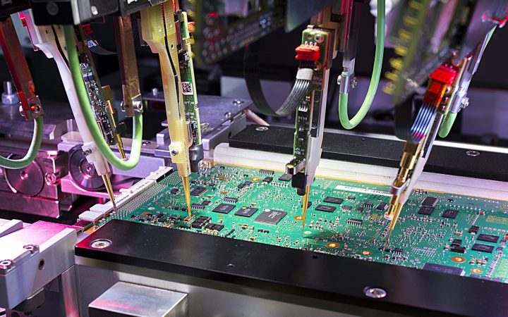
This test, performed after the assembly stage, verifies the correct functioning and position of each electronic component on the PCB. The test includes verification of short circuits, open circuits, resistance, capacitance and other parameters. For this purpose, a flying probe is used, composed of an array of drivers and sensors that perform the measurements required by the test by moving freely on the board. The probe is controlled by appropriate software, which can be modified by adapting the same test system to boards with different layouts. Alternatively, a test fixture can be used, consisting of a bed of nails designed for the specific DUT (Device Under Test). Each "nail" behaves like a real sensor, able to electrically connect a specific point of the DUT to the test system. Bed-of-nails is an expensive and not very flexible technique (each board requires its own bed-of-nails); moreover, it shows some difficulties in testing boards with high component density, where spacing between pins is reduced. The ICT technique has the advantage of detecting several defects, relating to both the individual components and their connections, and can be performed without powering the board. Its disadvantage is related to the cost (complexity of both bed-of-nails and control software) and the inability to test the connectors, a significant limitation in analog and digital systems consisting of multiple cards. Figure 2 shows an ICT test machine with a flying probe.
A simple protocol detailing a method to create a fluorescent test sample that can be used to measure the illumination uniformity of your confocal microscope.
A PCB is made up of different elements, each of which affects the overall performance of the electronic circuit. The minimum set of tests to be performed should include the following checks:
Security expert. I want to make an impact on a global basis. Sign Up · Organisation. I want to improve my threat detection coverage and reduce costs. Schedule ...


 Ms.Cici
 8618319014500