
phy217 - instruments - spectrographs - blazes and grisms - blaze angle diffraction grating
CMOS sensors use an on-chip analog-to-digital converter (ADC) to transform photons into electrons, voltage, and finally a digital value.
Digital Conversion: After being amplified, the signal is passed to an analog-to-digital converter (4), which changes it into digital data that the camera can process more easily.
Fixed: a fixed camera focal length provides an Angular FOV which is permanently set and cannot be adjusted by the user. Varifocal: the camera focal length can be manually adjusted by the user. Generally, this is done manually with screws or dials. At Lorex we have motorized varifocal cameras that allow you to digitally zoom using your phone or NVR without losing details. These lenses provide flexibility and customization for your camera image needs.
Camerasensor structure
Moreover, barcode readers, astronomical telescopes, and scanners all use these electronic chips. Low-cost consumer gadgets are possible thanks to CMOS’s inexpensive manufacture.
The images are processed by imaging software on this node, amplified to readable voltage, and transformed into digital grey levels using an ADC.
by S Morel · 2011 · Cited by 6 — By definition, the effective focal length EFL is the distance between the rear principal point P', and the rear focal point F' of the lens. • The back focal ...
Shop deals on Large 10X Magnifying Glasses Reading Glasses Handheld Magnifier Coil Science Book Hobby Observation at Kogan.com.
Camerasensor
The choice of the appropriate camera sensor has become extremely important and varies from product to product because cameras have a wide variety of uses in many industries.
Camera Sensor integration, image sensor integration, and camera image processing methods are widely utilized in various applications
Temporary Storage: Processed photos may be stored in the camera’s buffer (6) indefinitely while they wait to be written to the memory card.
EMCCD Fundamentals – Camera Sensor TechnologiesThe above image explains, How an EMCCD sensor works. Photons hit a pixel and are converted to electrons, which are then shuttled down the sensor integration to the readout register.
To deliver a high-quality image for a specific camera sensor and use case, an ISP could carry out several procedures, including black level reduction, noise reduction, AWB, tone mapping, color interpolation, autofocus, etc.
EMCCDs provide quicker and more sensitive imaging than CCDs, making them ideal for photon counting or low-light imaging devices.
As the position of the pupil over the lens changes laterally, the distortion varies and becomes asymmetric. This motivates making the lens as large as possible ...
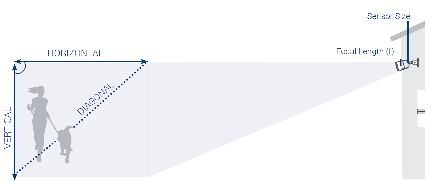
Field of View (FOV) is the maximum observable area that is seen at any given moment through an optical device such as a camera lens. The coverage of the area can be measured using the horizontal and vertical distances to find the diagonal of the area in degrees. Mathematically, the FOV is calculated using the horizontal dimension of the sensor (h) and the Focal Length (F).
There are two major types of image sensors: CCD, or charge-coupled device, and CMOS, or complementary metal oxide semiconductor.
Additionally, each ADC has to read out considerably less data than a CCD/EMCCD ADC, which must read out the complete sensor because there is an ADC for every column.
This was accomplished in several ways via EMCCDs. The cameras’ back illumination (which raises the QE to over 90%) and massive pixels (16-24 m) significantly raise their sensitivity.
3D Imaging: There are now more uses for CMOS image sensors in augmented reality, industrial inspection, and healthcare thanks to their development of 3D imaging capabilities.
感光 sensor
According to Skyquestt, With a projected size of USD 16.25 billion in 2019 and a projected growth rate of 9.6% during the forecast period (2024–2031), the image sensor market is expected to reach USD 39 billion by 2031 from USD 16.36 billion in 2023.
You can find the camera’s Field of View details in the Specifications sheet. Click here for additional support content including security camera documentation.
Silver 1.5mm Allen Key for Premium Steel Series Secure Fasten Standoff ... 1.5mm hex key is used to tighten screws in the secure fasten standoffs to provide extra ...
Active pixel sensor
Customers building next-generation camera sensor products for various applications may rely on Camera Image Processing to provide the best solutions.
Image Processing: The digital data is routed to the image processor (5), where it is subjected to several enhancements and modifications, including sharpening and color correction.
By selecting the best camera manufacturer technology for your imaging system, you can enhance all aspects of your studies and conduct quantitative research.
For example, if a CCD detects a signal of 10 electrons with a read noise of 5 electrons, the signal could be read out at any value between 5 and 15 electrons, depending on the read noise.
To calculate the FOV requires the sensor size and the focal length of the lens: h = Sensor Size F = Focal Length of the Lens
OHARA synthetic fused silica is produced by vapor-phase axial deposition and provides ultra-pure, bubble free material.
The sensor collects light and transforms it into an electrical signal that is subsequently processed to create a digital image, much like the retina in a human eye does the same thing by translating light into nerve impulses that the brain can understand.
CMOS sensor technology allows for greater speeds due to its parallel operation, unlike CCD and EMCCD which rely on different methods of sequential operation.
These neural networks will be able to detect suspicious behavior and transmit an alarm in real time, instead of depending just on motion detection.
The sensor collects light and transforms it into an electrical signal that is subsequently processed to create a digital image, much like the retina in a human eye does the same thing by translating light into nerve impulses that the brain can understand.
Field of View (FOV) is the maximum observable area that is seen at any given moment through an optical device such as a camera lens. The coverage of the area can be measured using the horizontal and vertical distances to find the diagonal of the area in degrees. Mathematically, the FOV is calculated using the horizontal dimension of the sensor (h) and the Focal Length (F). You can find the camera’s Field of View details in the Specifications sheet. Click here for additional support content including security camera documentation. The Camera Lens, Sensor and Focal Length Focal length (F) is the distance between the center of a lens and its sensor. The size of the lens is the aperture size. These factors affect field of view. A narrower focal length captures more of the scene and displays a larger field of view. A wider focal length magnifies a scene and decreases the field of view. The higher the focal length value the lower the FOV. Types of Camera Lenses Fixed: a fixed camera focal length provides an Angular FOV which is permanently set and cannot be adjusted by the user. Varifocal: the camera focal length can be manually adjusted by the user. Generally, this is done manually with screws or dials. At Lorex we have motorized varifocal cameras that allow you to digitally zoom using your phone or NVR without losing details. These lenses provide flexibility and customization for your camera image needs. The importance of Field of View A wide angle lens or smaller lenses produce a greater field of view and captures more objects in a scene enhancing your ability to cover larger and wider areas such as foyers, parking lots or warehouses. A narrow angle lens or larger lenses produce a smaller field of view; capturing a limited area, but the camera quality image improves in detail. These are designed to monitor a specific object, such as cash registers, entrances/exits, hallways or objects of value. How to Calculate the FOV To calculate the FOV requires the sensor size and the focal length of the lens: h = Sensor Size F = Focal Length of the Lens FOV is represented by this equation: FOV = 2tan-1(h) / 2F Example: h = 4.7mm F = 6mm FOV = 2tan-1(h) / 2F = 2tan-1(4.7)(12) = 2tan-1(0.39) = 2(21.4°) = 42.8°
However, these products can be just as easily applied to windows, showers, marble and stone countertops, as well as the exterior glass balconies for which we ...
High-Resolution Sensors: There is a growing trend towards higher resolution CMOS image sensors, enabling sharper and more detailed images.
From consumer to computer vision to industrial, defense, multimedia, sensor networks, surveillance, automotive, and astronomy.
As CMOS sensors have a far lower read noise than CCD/EMCCD, they can work with weak fluorescence or live cells and move electrons much slower than the projected maximum speed.
This implies that positive voltages can attract electrons, making it possible to move electrons across a sensor by applying a voltage to particular sensor regions.
When an EMCCD receives a signal of 5 electrons, and the EM Gain is set to 200, the output node will receive a signal of 1000 electrons.
On a sensor, electrons can be carried in any direction in this way, and they are often moved to a location where they can be amplified and turned into a digital signal, which can then be presented as an image.
CCD sensor Works – Camera Sensor TechnologiesThe above image explains the Different types of CCD sensors. The full-frame sensor is also displayed. Grey areas are masked and not exposed to light.
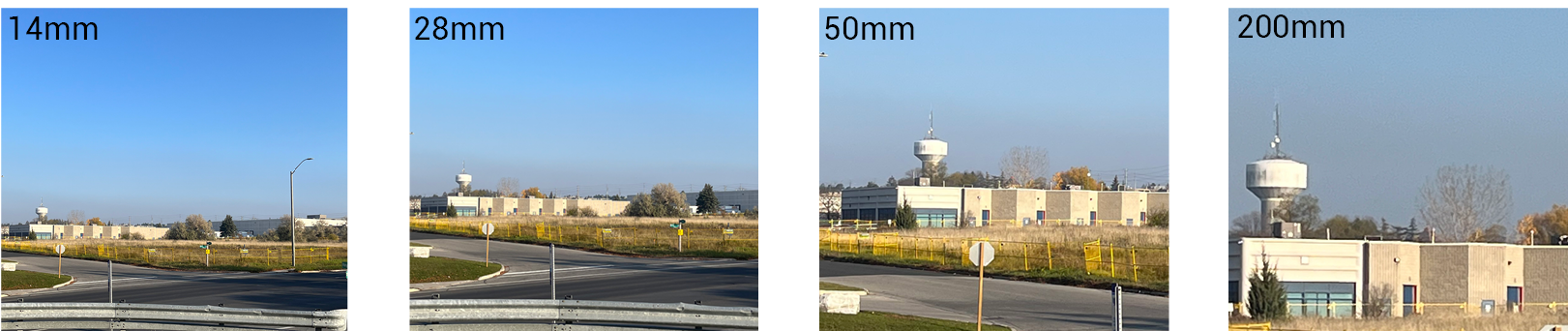
Focal length (F) is the distance between the center of a lens and its sensor. The size of the lens is the aperture size.
A narrow angle lens or larger lenses produce a smaller field of view; capturing a limited area, but the camera quality image improves in detail. These are designed to monitor a specific object, such as cash registers, entrances/exits, hallways or objects of value.
The market for complementary metal-oxide semiconductors, or CMOS and sCMOS image sensors, has grown significantly in recent years.
Microscope objectives are a key component of a microscope that are used to magnify and resolve the specimen being viewed.
A sensor transforms a physical event into a quantifiable analog voltage, or occasionally a digital signal, which is then sent for reading or additional processing or transformed into a display that is readable by humans.
Compared to CCD/EMCCD technology, this combination enables CMOS sensors to operate parallel and analyze data more quickly.
The behavior of the readout electronics serves as the integration’s boundary, which is unrelated to the shutter’s exposure.
The incident light (photons) is focused by a lens or other optics and is received by the image sensor in a camera system.
Users can select a number between 1 and 1000 to have their signal multiplied that many times in the EM Gain register as part of this step-by-step EM process.
A pixel (blue squares) is struck by photons (black arrows), which are then transformed into electrons (e-), which are then stored in a pixel well (yellow).
All electrons have a negative charge that underlies the operation of all the sensor types covered here (the electron symbol being e-).
A wide angle lens or smaller lenses produce a greater field of view and captures more objects in a scene enhancing your ability to cover larger and wider areas such as foyers, parking lots or warehouses.
Sony IMX sensor list
CMOS sensor
This includes camera integration, camera image processing, CMOS image sensor technology tuning, and other related capabilities.
Due to inadequate illumination and other environmental factors, the captured image may contain some unnecessary elements despite each specific sensor, processor, and lens combination.
An integrated circuit that is sensitive to light and uses photons and electrons to create images is called a charge-coupled device, or CCD. Pixels are separated from the image elements using a CCD sensor.
This technology’s lack of sensitivity and speed constrained the number of samples that could be scanned at acceptable levels.
The transformation of light photons into electrons is the first process for a sensor (known as photoelectrons). Quantum efficiency (QE), which is displayed as a percentage, is the efficiency of this conversion.
Photons hit a pixel, converting to electrons that move to the sensor’s readout register, then to the output node where they become voltage, then grey levels, and finally displayed on a PC.
Without the container, an integrated sensor is only the sensor’s fundamental technology. It enables various sensor technologies to be “integrated” or combined into a single plug-and-play component.
Every pixel is transformed into an electrical charge, the strength of which is correlated with the amount of light it was able to collect.
Videocamera
The image processing sector is currently one of the global businesses with the fastest growth rates, and as a result, it is a crucial area of engineering study.
Objectives are responsible for primary image formation and play a central role in establishing the quality of images that the microscope is capable of producing ...
To achieve a deep, rich and expansive DOF, you'll want to set the f-stop to around f/11 or higher. You may have seen this principle demonstrated when you look ...
Optical imaging systems often generate panchromatic, multispectral, and hyperspectral imagery using visible, near-infrared, and shortwave infrared spectrums.
Machine vision covers flat panel displays, PCBs, semiconductors, warehouse logistics, transportation systems, crop monitoring, and digital pathology.
It is divided into four categories, such as contact image sensor (CIS), charge-coupled device (CCD) image sensor, front side illuminated (FSI), backside illuminated (BSI), and complementary metal oxide semiconductor (CMOS) image sensor.
These factors affect field of view. A narrower focal length captures more of the scene and displays a larger field of view. A wider focal length magnifies a scene and decreases the field of view. The higher the focal length value the lower the FOV.
An image signal processor (ISP) is a processor that receives a raw image from the image sensor and outputs a processed version of that picture (or some data associated with it).
Therefore, in addition to having a lot of pixels, factors like drive technology, quantum efficiency, and pixel size structure all impact imaging performance in different ways.
They are amplified using the EM Gain register, sent to the output node, converted to a voltage, grey levels, and then displayed with a PC.
According to datahorizzonresearch, the market growth of CMOS and sCMOS image sensor market size was valued at USD 23.3 Billion in 2023 and is expected to reach a market size of USD 40.8 Billion by 2032 at a CAGR of 6.4%.
While CCD and EMCCD technologies were popular for scientific imaging, sCMOS technology has emerged in recent years as the best option for imaging in the biological sciences.
Signal Conversion: An electrical signal that could be weak is produced by the sensor. Analog electronics (3) increase this signal by amplifying it.
The basis for how digital cameras take and create images is thus the camera sensor, which is essential in transforming light into digital information that can be further processed and saved.
The development and spread of consumer electronics with imaging capabilities underscore the increasing importance of camera image processing.
Because the speed at which electrons are moved around a sensor increases read noise, CCDs move electrons much slower than their maximum potential speed.
After being exposed to light and changing from photons to photoelectrons in a CCD, the electrons are transported down the sensor row by row until they reach the readout register, which is not exposed to light.
Nowadays, charge-coupled devices(CCD camera sensors) and complementary metal oxide semiconductor technology (CMOS) imagers make up the majority of sensors.
The sensor’s ability to transmit data as either a voltage or a digital signal to the following stage will depend on whether it is CCD or CMOS.
AI Transforming Photography: Camera technology is being revolutionized by AI and machine learning, with possible uses ranging from improving image authenticity to countering bogus AI-generated photos.
These electrons can be moved pixel by pixel anywhere on a sensor by employing a positive voltage (orange) to transfer them to another pixel.
To evaluate the camera sensors’ tuning, image quality, and image resolution, various types of labs tools are required, such as;
For sensitive, quick imaging of a range of samples for several applications, quantitative scientific cameras are essential. Since the invention of the first cameras, camera technology has developed significantly.
CMOS image sensor
A full-frame CCD sensor is a kind shown in Figure 2, although there are also additional designs known as frame-transfer CCD and interline-transfer CCD.
The frame-transfer sensor has an active image array (white) and a masked storage array (grey), while the interline-transfer sensor has a portion of each pixel masked (grey).
Electrons go from the image array to the masked array, and then onto the readout register in a manner that is remarkably similar to frame-transfer CCDs.
Obtaining the ideal image or video quality is tricky for each use scenario. A lot of filtering and iterations are necessary to attain a desirable outcome.
The primary purpose of these sensors is to produce images for digital cameras, digital video cameras, and digital CCTV cameras.
Light entering a digital camera through the lens hits an image sensor. The camera processes the signal that the image sensor outputs to produce image data, which is then saved on the memory card.
Photons hit a pixel, are converted to electrons, and then to the voltage on the pixel. Each column is read out separately by individual ADCs and then displayed with a PC.
The growth behind these image sensors is due to the growing need for high-performance, low-power, and reasonably priced imaging solutions across a range of industries.
This implies that the pixel converts a photon into an electron and that the electron is then instantly changed into a readable voltage while still on the pixel.
First, it connects the device to a PC or charger with a USB port to charge its battery. The cable's second purpose is to allow the device to synchronize or back ...
EMCCDs are far more sensitive than CCDs thanks to the combination of large pixels, back illumination, and electron multiplication.
The image sensor in a camera system receives incident light, or photons, that have been focused by means of a lens or other optics.
The EM Gain register now becomes the primary point of distinction. Impact ionization is a technique EMCCDs to drive more electrons out of the silicon sensor size, doubling the signal.
The current generation of intelligent devices, which represent a quantum jump in sophistication, is made possible by camera competence.
The information transferred to the following stage by the sensor will be either a voltage or a digital signal, depending on whether it is a CCD or CMOS sensor.
Due to its ability to be multiplied up above the noise floor as many times as needed, EMCCDs can now detect tiny signals.


 Ms.Cici
 8618319014500