
Group Velocity Dispersion (GVD) - group velocity dispersion
CMOSvs CCD
Achieve a wide variety of artistic effects, from light trails to smoothing water and moving subjects with perfect color accuracy.
When both types of sensors come with their own set of advantages, CMOS sensors have started becoming more popular in recent years, especially in the embedded vision space. While a vast majority of the discussions around the comparison of these two technologies have revolved around mobile phone cameras and machine vision systems, not much has been spoken about the topic in light of embedded vision.
Types ofcmos in camera
While things are dark on the CCD side, the future looks shiny for CMOS sensors. From global shutter to extreme low light cameras to high-resolution cameras, advancements are moving fast in CMOS technology. With leading sensor manufacturers such as Sony, Onsemi, Omnivision etc putting more focus on enhancing the sensitivity, resolution, dynamic range, power efficiency, etc of CMOS sensors, innovations in the space are happening with lightning speed.
CMOSfull form
Hope you were able to develop a good understanding of CMOS and CCD technologies and the key differences between the two types of sensors. If you have any further queries on the topic or are looking for help in integrating a CMOS camera for your vision-based application, please write to us at [email protected].
In this article, we briefly look at some of the key differences between CMOS and CCD sensors, why CMOS is gaining on – or is already beating– CCD in embedded vision, and what the future holds for both in the imaging world.
cmossensor vs full-frame
CMOS stands for ‘Complementary Metal Oxide Semiconductor’. The major difference between a CMOS and a CCD sensor is that the former has an amplifier in every pixel. In some CMOS sensor configurations, each pixel has an ADC as well. This results in higher noise compared to a CCD sensor. However, this setup makes it possible to read several sensor pixels simultaneously. In a later section, we will also see how CMOS sensors are matching CCD’s performance despite having this disadvantage.
Moreover, many imaging applications like medical microscopy that stayed with CCD for much longer compared to other embedded vision applications have also joined the ‘CMOS wave’. Further, in addition to power consumption advantages, CMOS sensors also tend to offer higher frame rates and better dynamic range. This has also led embedded camera companies to come up with cutting-edge camera solutions using CMOS sensors. For instance, e-con Systems’ wide portfolio of CMOS cameras includes a 16MP autofocus USB camera, 4K HDR camera, global shutter camera module, IP67 rated Full HD GMSL2 HDR camera module, IP66 rated AI smart camera, and much more (To get a complete view of e-con Systems’ CMOS camera portfolio, please visit our Camera Selector).
With further developments stalled, we are soon likely to see the death of CCD sensors. In fact, many sensor manufacturers had already stopped producing CCD sensors years back, but are merely continuing to support their existing customers using them.

CCD sensors remained the natural choice for many product developers for a very long time when it came to building camera-based devices that need to operate under low lighting conditions or an IR/NIR light source. This was true especially in higher temperature ranges where CMOS sensors needed an additional cooler to maintain the required level of QE (Quantum Efficiency – a measure that indicates the sensitivity of a sensor). This was also owing to the fact that CCD sensors offered the flexibility of having a thicker substrate layer for the absorption of photons in the NIR spectrum. But recent developments in the CMOS sensor technology have given birth to sensors that offer better sensitivity than traditional CCD sensors. For instance, the STARVIS series from Sony includes a wide variety of sensors with superior low light performance and NIR sensitivity.
CMOSsensor
The invention of image sensors dates back to the 1960s. A journey that started with designing the MOS (Metal Oxide Semiconductor) sensor architecture in the early 1960s and developing the first digital camera in 1969 to the latest SPAD (Single Photon Avalanche Diode) technique from Canon, sensor technology has come a long way. Despite these developments, CCD and CMOS sensors have remained two of the most popular sensor technologies in the imaging space for decades.
CMOSimage sensor working principle
ND filters allow videographers to dial in exposure in any lighting condition so they can shoot wide-open with shallow depth-of-field.
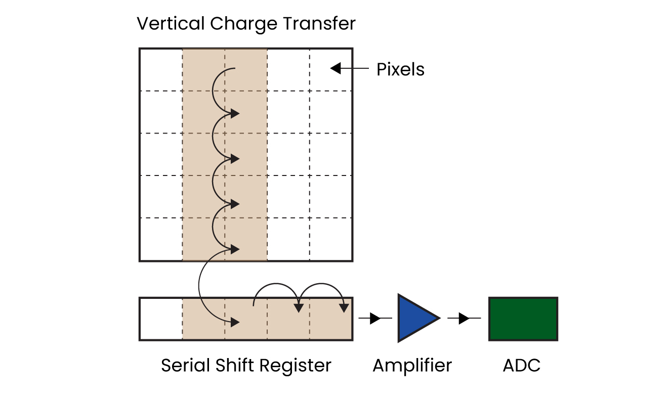
A CCD sensor is an analog device. Below the CCD layer lies the SSR (Serial Shift Register) which is connected to an amplifier on one end and an ADC (Analog to Digital Converter) on the other. The charge in the CCD layer is transferred to the SSR, and then to the amplifier and the ADC. This charge is read from each pixel site to recreate the image. Have a look at the below diagram to understand how the whole process works:
Cmos in cameraiphone
Both CCD and CMOS technologies use the photoelectric effect to convert packets of light (or photons) into electric signals. Also, these two sensors are made up of pixel wells that collect these incoming photons. The fundamental difference between the two lies in recreating an image from electric signals.
As discussed before, CMOS cameras are catching up on CCD cameras when it comes to most of the imaging parameters. Reduced costs with matching performance are encouraging more and more product developers to pick CMOS sensors over CCD sensors. Also, for the same reason, sensor manufacturers are also gradually moving away from developing new CCD sensors. Hence not much research or advancement is happening in the space. This is resulting in a cascade effect that is reducing the popularity of CCD sensors over time.
Neutral Density Filters have an evenly distributed coating throughout the lens that provides light filtration by a certain degree of strength. The strength of the filter can be referred to by f-stops. They range from 3-stops which filters out about half of the available light to 16.6-stops which let through only 1/32,000ths.
In a CCD sensor, when photons get converted into electric signals, the charge to be converted into voltage is transferred through a limited number of nodes. This would mean that only a few amplifiers and ADCs are in action, which in turn results in less noise in the output image.
This blog post was originally published at e-con Systems’ website. It is reprinted here with the permission of e-con Systems.
Here you’ll find a wealth of practical technical insights and expert advice to help you bring AI and visual intelligence into your products without flying blind.


 Ms.Cici
 8618319014500