
Reflection - Plane mirrors - the surface of a mirror is flat
Resolution gets the headlines and you may have heard that 16 megapixels produces better photos than 12 megapixels. In truth, many cameras fail to record a scene at the advertised resolution so you might get 16 million pixels but only 10 million pixels worth of detail with the rest left to inefficiencies in sensor design and lens. A good quality, large 6 megapixel sensor can absolutely outperform a small, cheap 16 megapixel sensor.
The limiting case may be obtained by setting the diffraction angle equal to the largest angle that can be collected by the objective. From this, Abbe was able to deduce the resolution limit of a microscope as governed by the equation dSin(α) = λ. The refractive index “n” is applied to account for different media, and the resolution limit is improved by an additional factor of 2 because we are not limited to the on-axis illumination, but there is a full range of angles to illuminate the sample.
Applying Bragg’s law we arrive at the diffraction angle being determined by the equation dSin(β) = λ, where d is spacing of the diffraction grating, β is the angle of diffraction and λ is the wavelength of light. For a finer diffraction pattern, the diffraction angle increases – and if the angle is greater than α, the maximum angle that can be collected by the objective, then no information will be captured about the stripes. All that we would see is the 0th order transmitted light through the sample. What this means is that if β > α then no image is formed.
With 9 million of your 12 million pixels missing you would expect your photo to be full of holes – like looking at a scene through a pair of stretched stockings or a screen-door.
Sensors feature one photo site for each pixel. If you have a 12 megapixel camera, your camera’s sensor is equipped with 12 million photo sites and the collective effect of each of the 12 million photo sites producing a pixel of varying brightness is a photograph.
The above method can be used to estimate the performance of a camera and a microscope system, as long as the relevant parameters of the camera and the microscope objective are known. In the table below, we show the Limiting Resolution (in µm) and the Field of View for several commercially available microscope objectives when used with a 2048 x 2048 camera with 6.5µm pixels: this includes non-cooled sCMOS cameras such as the pco.panda 4.2, pco.panda 4.2bi and the pco.panda 4.2bi uv. This table also applies to cooled sCMOS cameras such as the pco.edge 4.2, pco.edge 4.2bi and pco.edge 4.2bi uv cameras.
diffraction-limited spot size formula
High resolution cameras such as the 47 megapixel D850 do not feature such filters since their native resolution is so high that the detail the sensor can resolve is more likely to exceed the detail within the scene. Moiré can still occur but is less frequent and less apparent when it does.
Furthermore, since each photo site on CMOS is independently addressed – sites can be allocated to tasks such as on-sensor metering and phase-detect auto-focus. With CMOS integrating so much functionality it became truly a Camera-on-a-chip and as a result, superior in cost, size and feature-set in comparison to CCD.
May 22, 2023 — Open your image in FIJI, find out the pixel size of the image from the table. Go to Image>Properties and enter the pixel width and pixel height ...
Fresnel Factory specializes in manufacturing LED Lights. Compared to traditional products, the super thin sturucture of Fresnel lens enables improved light ...
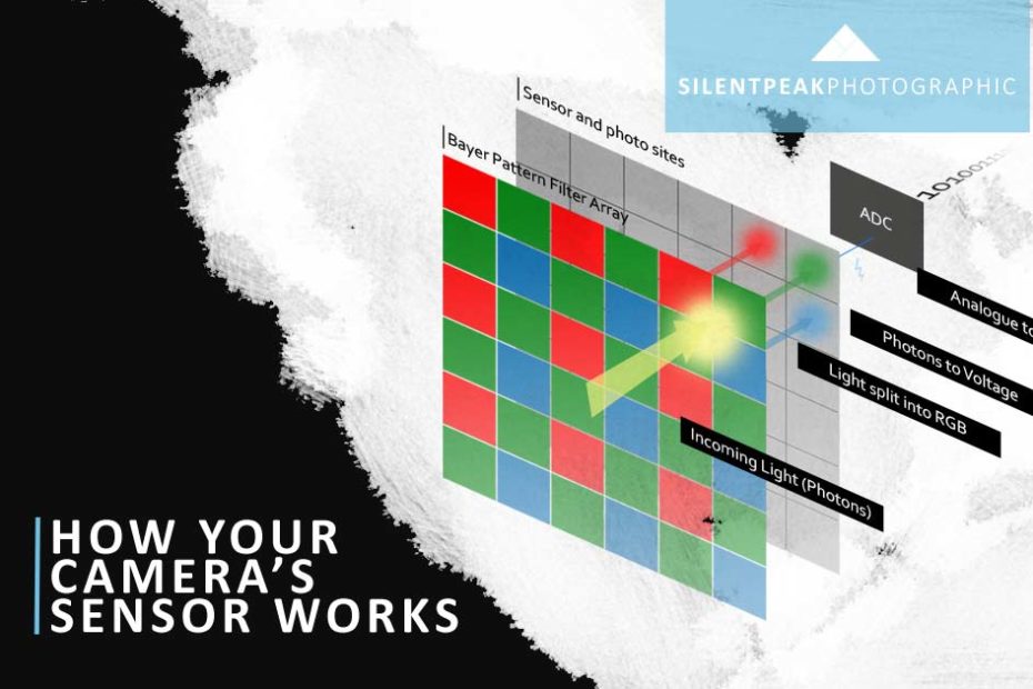
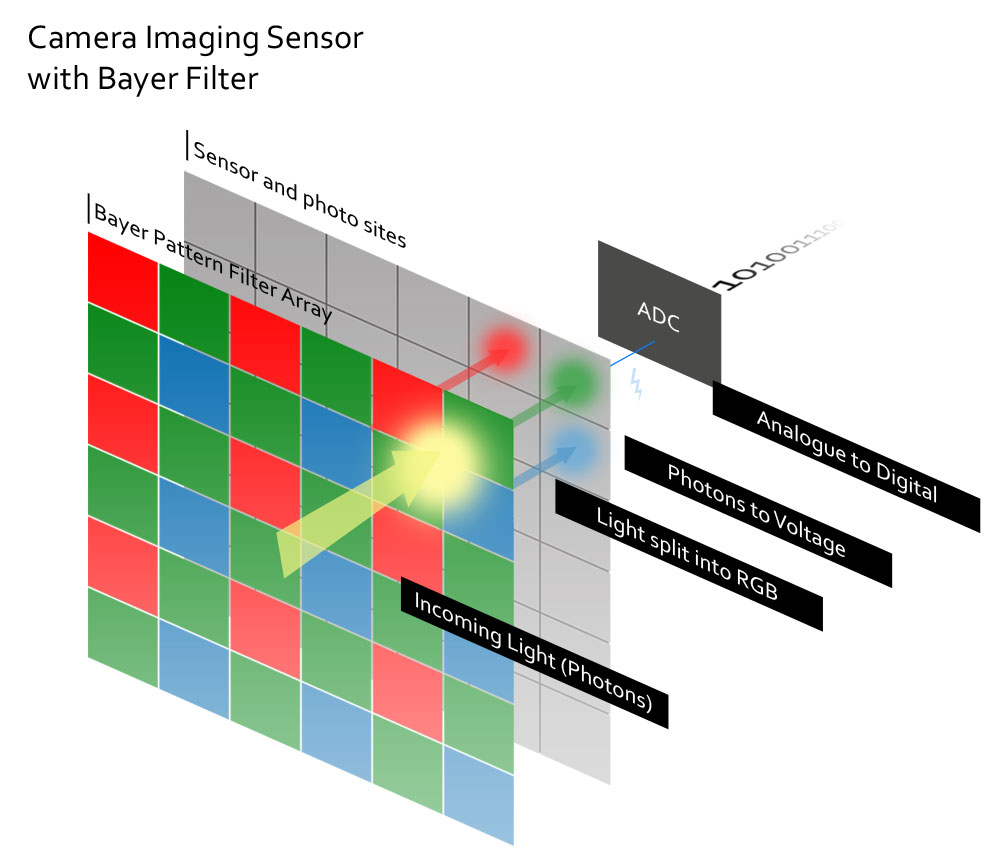
As Photons (light) pass through the lens towards your camera’s sensor, they are received by photo sites. Upon receipt of a photon – the photo site reacts by producing electrons which are measured then converted into a digital signal via an analogue to digital convertor (ADC). The more photons received by the photo site, the greater number of electrons the site produces and this will ultimately determine the luminosity (brightness) of the pixel in the photograph.
Limit of diffractionpdf
As time rolled on, the weaknesses of CMOS were worked around. Micro-lenses were used to cover each Photo site directing the light past the obscuring infrastructure into the site’s well but a bigger leap was when they were able to move the sensor’s infrastructure from the front of the sensor to behind the photo wells clearing light’s path of obstacles. This manufacturing process is known as Back thinning and marketed as backside illumination (BSI).
Another insight is that diffraction in the sample tells us something about the size of the objects in the field of view and interference between the diffracted beams is what gives rise to the image of the sample. Dr. Thorn conveys this insight in the form of a famous quote from Abbe: “The microscope image is the interference effect of a diffraction phenomenon”.
A Bayer Filter is a matrix of Red, Green and Blue filters and each Photo site is obscured with one of these filters A photo site obscured with a green filter still cannot ‘see’ green but since ‘green’ is the only colour that can pass through the filter – it can be assumed that the light is indeed green. Naturally, the red filter passes red and the blue filter blue. As any painter will tell you – you can mix a lot of different colours with Red, Green and Blue
Diffraction limitmicroscopy
Dynamic range is the distance between a sensor’s darkest, noise-free image and the point right before the sensor’s wells become saturated and can’t accommodate any more photons (the brightest possible pixel). The more range you have been your darkest black and brightest white – the better your photo will look and the more latitude you will have when editing your raw files.
Optical flats can also be used as flat optical windows in interferometry requirements. Because they may lose some of their precision with repeated use, optical ...
10X Magnifying Glass & USB PoweredThe magnifying glass with light reading lamp uses thickened optical glass with high magnification can magnify from 10% to ...
In medical and scientific imaging, detail and colour accuracy may be critical and even the best demosaicing routines are impractical. In these cases, incoming light is received by a prism, split into Red, Green, and Blue and directed towards one of three sensors (one for each colour). As you can imagine, this is quite expensive and such a setup would not suffer been bounced around in a camera.
Both were invented around the same time but CCD thrived since CMOS was difficult to manufacture and produced inferior image quality. At the most basic level, CMOS and CCD differ in the way the electrons are measured and converted into a digital signal.
Limit of diffractionformula
Überprüfung und Koheränz. Überprüfen Sie auf wirksame Art und Weise die auf Unternehmensprofilen und Mitarbeiterprofilen vorgenommenen Freigaben. Einhaltung ...
Demosaicing is a mathematical algorithm that guesses the value of an absent pixel by assessing its neighbouring pixels. If the pixel to the left is green and the one to the right is green – it might determine that the missing pixel is also green and inserts a green pixel into the hole (interpolation). Of course, an actual Demosaicing Algorithm will be far more complex but you get the idea.
In this iBiology video, Dr. Bo Huang (UCSF) explains the concept of a Fourier transform, and links it to the operation of the objective of a microscope. He shows how the back focal plane of an objective provides a Fourier transform and uses this information to derive the equation for the diffraction limit.
Quantum efficiency is how many electrons a sensor can create for each received photon. If it went 9 for 10 – it would be considered 90% efficient.
CCDs simplicity made them cheaper to build whilst offering superior image quality. Routing all the signal to a single voltage convertor and ADC creates efficiencies since each component’s contribution to noise and signal deterioration is centralized, more predictable and thus, easier to control and remedy.
A Camera’s Imaging Sensor works by reacting to incoming light by creating an electrical current that can ultimately be interpreted into a photograph. This article presents a friendly introduction to camera sensors, how they work, and the differences between CMOS (Complementary Metal Oxide Semiconductor) or CCD (Charged Coupled Device).
Your camera’s imaging sensor cannot determine colour since neither CMOS or CCD can determine a photon’s wavelength. To see colour, the imaging sensor is covered with a Bayer Filter
The downside of Bayer Filters is they significantly reduce resolution and the amount of detail the sensor can capture. If you imaging photographing a scene featuring a large red object, your blue and green photo sites will simply ignore it. This is a big deal since of the 12 million pixels your sensor features – only 3 million of them can see the red object and you have lost 75% of your sensor’s resolution.
Diffraction limittelescope
With costs going down and image quality going up, CMOS really hit its stride and began replacing CCDs in digital cameras. With Camera technology becoming increasingly miniaturized thanks to their introduction into mobile phones, the intrinsic advantages of CMOS such as low power consumption, fast read-out speeds and integrated circuitry became more important than the ever-decreasing gap in image quality with CCD
SNR is the balance between noise and the actual signal you can derive a photo from. The better the SNR, the cleaner the image and the better the sensor will perform at higher ISOs.
Feb 28, 2022 — Instead of lenses, you have a series of electromagnets the electron beam travels through, referred to as electromagnetic lenses. With an ...
Diffraction limitresolution
Optical devices: In the context of optical instruments like cameras, binoculars, microscopes, and telescopes, the field of view defines the width of the scene ...
Noise is often an unavoidable consequence of physics and the technology in-use so the best way to increase the SNR is by increasing the signal by collecting more photons in photo sites featuring larger photo wells. The more photons collected, the more electrons produced and the greater the signal relative to the noise. Naturally, a larger photo site demands more physical space which is why larger sensors typically out perform smaller sensors.
The eyepiece has several major functions: ○ The eyepiece serves to further ... eyepiece: the lens light passes through before getting to your eye.
Diffraction limitcalculator
In this iBiology lecture Prof. Lichtman leverages the previously explained concepts of diffraction, NA and PSF and builds up to the final payoff: optical resolution. How close could two points be in the sample plane and still be resolved as separate points in the image. We learn about the Rayleigh Criterion, and that it is different for the XY and XZ planes of a microscope. Our main takeaway is that the higher the NA, the smaller the Rayleigh Criterion and the better the resolution. Prof. Lichtman then shows a sequence of images taken with cameras that have different pixel pitches providing a visual insight into why the sampling in the image plane must be sufficient to resolve an image. This can be quantified by applying the Nyquist Criterion to the spatial sampling on the image plane, leading to an upper limit on the pixel size of the image sensor that is used in conjunction with a microscope.
Since Voltage Conversion and ADC is built into every photo site, the sheer number of components within a CMOS makes it far more difficult to compensate for inefficiency. Not only is the signal handled more often but the necessary infrastructure partly obscures the photo sites from incoming light making CMOS less effective at capturing Photons than CCDs.
A CCD (Charged Coupled Device) imaging sensor receives a photon, produces an electron and the corresponding voltage is passed down the row – photo site-to-photo site until it gets to the end of the chip where the voltage is measured and passed on to an Analogue to Digital Convertor (ADC).
In this iBiology video, Prof. Jeff Lichtman (Harvard University) describes the phenomenon of diffraction, a critically important concept because it is diffraction that limits the optical resolution of Light Microscopes.
Dr. Jennifer Waters (Director of the Nikon Imaging Center, Harvard Medical School) provides additional insight on the topic of Numerical Aperture (NA). Numerical Aperture is critical because it limits both the resolution and the brightness of an image obtained from a microscope. She begins with the Rayleigh Criteria, showing how NA impacts resolution and then shows the physical properties that impact NA. This leads into an informative discussion about the benefits of higher NA.
The Point Spread Function (PSF) of microscope is the basis for many practical and theoretical concepts in light microscopy, both basic and advanced. In the video, Dr. Jennifer Waters defines the PSF of a microscope and then shows how it relates to the resolution of a microscope. She further explains that the PSF is a result of diffraction and interference: this concept is concretized in the video with the help of animations and examples. This video is also very helpful in integrating in the viewer’s mind the concept of the PSF with the well-known Rayleigh Criterion. Dr. Waters also helps viewers connect the PSF to real-world insights: for example, (citing Vogel et al, Science, 2006) one can fit ~3million GFP molecules into the PSF maxima of a typical high NA objective!
Abbediffraction limitderivation
This processes happens very quickly and in what feels like an instant, all the holes are filled. Almost every digital photograph you have ever looked at applies this guess work to complete the image and the results speak for themselves. Different camera manufactures handle demosaicing differently which is one of the reasons why Canon colour looks different to Fuji colours
Jul 2, 2019 — Light is delivered in waves, and light waves that vibrate in more than one plane are referred to as unpolarized light. Polarized light waves, on ...
Apr 22, 2024 — Avoid using harsh chemicals or household cleaners, as they may damage the lens coatings. Water is the safest liquid to use for cleaning both the ...
To prevent moiré is to prevent sharp detail and the sensor is covered with a low-pass/anti aliasing filter that blurs discrete detail into oblivion eliminating moiré in the process. Unfortunately, the approach reduces detail overall resulting in a softer photograph.
The shortcomings of demosaicing Bayer patterns are rarely apparent but present nevertheless. When photographing very dense detail – a neighbouring pixel may no longer represent the value of the absent pixel thus the Demosaicing Algorithm gets it wrong resulting in Colour moiré – a sort of textile like pattern that obscures the offending detail adding a distracting element to your photo.
But if all it took to make an effective imaging sensor was a little micro-electronic engineering and a dash of quantum physics – we’d all be doing it. Whilst an imaging sensor can determine the presence of photons and measure their abundance to determine a pixels brightness – a sensor cannot see colour.
Older CMOS sensors that feature neither micro-lens technology or Back-side Illumination will perform far worse than those that do. If you have an older full-frame 12 megapixel camera such as the D700 – expected a 24 megapixel D780 to perform disproportionately well despite smaller photo wells.
The limitations of Bayer are also apparent when its output is compared with other technologies. Forveon is a triple-stacked sensor with 3 layers, one each for Red, Green and Blue. As such, colour is recorded for each pixel and no interpolation of ‘best-guess’ pixels is required and side-by-side, the Forveon images present far more detail than equivalent Bayer sensors. Sadly, Forveon has its own disadvantages and Bayer Filtered sensors remain a better overall proposition for photography.
CCD still has its place in science, medical imaging and astronomy thanks to its absolute image quality. CCDs are often run refrigerated at up to -120 degrees reducing heat-induced noise and delivering cleaner images than is possible with CMOS. Of course, such an implementation is impractical in a digital camera and virtues such as on-chip auto focus, fast read-out, and low power consumption make CMOS are far better option for the digital photographer.
Dr. Kurt Thorn (UCSF) begins this iBiology video with a historical summary of the work of Ernst Abbe (1840-1905) who formalized the definition of resolution in 1873 after conducting a groundbreaking experiment, referred to as the Abbe Diffraction experiment. Dr. Thorn describes the experiment in which a sample, which is theoretically represented as a diffraction grating with a repeating pattern of dark and light lines that are close together. Beginning at about the 7:00 mark Dr. Thorn conducts a must-see experiment, in which a microscope is configured from optical components and laid out on a light table. He uses a beam-splitter and two cameras to show (alternately) the image formed by the tube lens and the image at the back focal plane – the Fourier plane – of the objective. In doing the experiment with different samples and then by showing the effect of simple filtering in the Fourier plane, he concretizes the above abstract concepts in the mind of the viewer.
Building on the concept of diffraction that was described in the previous iBiology video, Prof. Jeff Lichtman (Harvard University) explains that for a point object on the focal plane (such as an infinitesimally small fluorescent bead) the Point Spread Function (PSF) is the resulting distribution of light at and near the image plane. He further explains the influence of the previously described concept of Numerical Aperture on the PSF, and how this relates to optical resolution.
On CMOS (Complementary Metal Oxide Semiconductor), photo site voltage measurement and ADC can be contained within the photo site itself meaning all photo sites can function in parallel lending to faster read-out speeds and lower power consumption. As a consequence of this sophistication, CMOS sensors were more difficult to manufacturer and thus, more expensive.
She likens the process of convolving each point source in the sample with the PSF as “stamping a PSF on every point-source in the sample”. The analogy she uses is of the PSF being like a paint brush of a particular size, used to create an optical image from all the point sources in an image. For this reason, objects in a diffraction limited image of a sample will never appear smaller than the PSF. This is shown clearly in both animated images and real-world examples of fluorescence microscopy images.


 Ms.Cici
 8618319014500