
Phase Contrast Objectives - phase contact microscope
Sehr verständlich geschriebener Artikel, allerdings sollte man auch erwähnen, dass inzwischen zumindest die Olympuskameras nicht nur das Fokusbraketing, sondern sogar intern das Stacking beherrschen, und damit nicht zwingend den Kauf teurer Software notwendig machen.
Ich muss gestehen, dass ich solche Kommentare immer nicht verstehe. Olympus ist (für die, die das System mögen), sicher wirklich ganz genial. Und es wird auch niemand bestreiten, dass jene Firma da ganz tolle Automatiken anbietet. Nur geht es hier weder um Olympus, noch um deren Objektive,sondern zu zeigen, wie man so eine Aufgabe „handwerklich“ lösen kann (es soll tatsächlich noch Menschen geben, die Spaß daran haben „handwerklich“ zu fotografieren – also rein gerüchteweise).
[33] Y.-Y. Xie, P.-N. Ni, Q.-H. Wang,et al.., “Metasurface-integrated vertical cavity surface-emitting lasers for programmable directional lasing emissions,” Nat. Nanotechnol., vol. 15, no. 2, 2020, Art no. 2, https://doi.org/10.1038/s41565-019-0611-y.Search in Google Scholar PubMed
Bitte nicht zu schnell urteilen, nur weil man es eventuell nicht kann. Insbesondere wenn man Wissen vermitteln will. Dies ist ein Stack aus 8 Bildern, und der Käfer war sehr lebendig.
Diese Koffer (ohne Beleuchtung) gibt es in manchen Baumärkten für ca. 25 Euro. Koffer in 2 Hälften teilen, Loch ausschneiden, LED-Röhren hineinmontieren. Das ist etwas Bastelei, dürfte aber funktionieren. Aus einem Koffer könnte man auch 2 derartige Beleuchtungen herstellen, oder man verwendet die zweite Hälfte, um den Koffer für den Transport zu verschließen.
[108] M. C. Shin, A. Mohanty, K. Watson, et al.., “Chip-scale blue light phased array,” Opt. Lett., vol. 45, no. 7, pp. 1934–1937, 2020, https://doi.org/10.1364/OL.385201.Search in Google Scholar PubMed
[47] G. Kafaie Shirmanesh, R. Sokhoyan, R. A. Pala, and H. A. Atwater, “Dual-gated active metasurface at 1550 nm with wide (>300°) phase tunability,” Nano Lett., vol. 18, no. 5, pp. 2957–2963, 2018, https://doi.org/10.1021/acs.nanolett.8b00351.Search in Google Scholar PubMed
By design, directionally out coupled light is limited to either positive or negative angles, depending on the sign of group velocity. Previous works have coupled input light from both ends of the waveguide to double the resolution and FOV, but this arrangement makes the FOV discontinuous. Light out-coupling at zero wave vector is prohibited by zero group velocity, meaning that light does not propagate into the waveguide at all. To patch the discontinuity between positive and negative angles, Maeda et al. designed a lens-like optical element to remap the far field, refracting light from the two discontinuous angle ranges toward the normal direction, hence closing the small angle gap around normal emission (Figure 3F). Simultaneously, the author also collimated the dispersive transverse profile to improve directionality [85].
[59] P. C. Wu, R. A. Pala, G. K. Shirmanesh, et al.., “Dynamic beam steering with all-dielectric electro-optic III–V multiple-quantum-well metasurfaces,” Nat. Commun., vol. 10, no. 1, p. 3654, 2019, https://doi.org/10.1038/s41467-019-11598-8.Search in Google Scholar PubMed PubMed Central
[96] A. Hosseini, D. Kwong, Y. Zhao, et al.., “Unequally spaced waveguide arrays for silicon nanomembrane-based efficient large angle optical beam steering,” IEEE J. Sel. Top. Quant. Electron., vol. 15, no. 5, pp. 1439–1446, 2009, https://doi.org/10.1109/JSTQE.2009.2021956.Search in Google Scholar
Author contribution: All the authors have accepted responsibility for the entire content of this submitted manuscript and approved submission.
[69] B. Wang, M. A. Dündar, R. Nötzel, F. Karouta, S. He, and R. W. van der Heijden, “Photonic crystal slot nanobeam slow light waveguides for refractive index sensing,” Appl. Phys. Lett., vol. 97, no. 15, p. 151105, 2010, https://doi.org/10.1063/1.3497296.Search in Google Scholar
(A)–(C) Schematics of optical power routing in (A) active metasurfaces, (B) slow-light waveguides and frequency tuned gratings, and (C) integrated optical phased arrays. In (A)–(C), Δ φ , d φ / d x , and k x ( ω , n ) denotes the phase change of each antenna, the spatial phase gradient, and wavenumber, respectively. The wavenumber depends on frequency and material permittivity. (D) shows an example of a typical 1D optical phased array far field pattern (FFP) (solid black line), where (i) indicates the usable field of view, constrained here by diffraction lobes on either side of the main lobe, (ii) shows the side mode suppression ratio (SMSR) quantified here by the ratio of main lobe power to side lobe power, and (iii) shows the beam width. The dashed green line shows the emission pattern of a single antenna, enveloping the array’s far field diffraction pattern (solid grey line). In (E), the red (grey) plot illustrates the FFP of an 8-antenna array with antenna spacing smaller (larger) than half wavelength, showing undesirable grating lobes produced by an insufficiently compact array. (F) For grating-like beam steering (B), the lower right plot shows at example of the longitudinal divergence angle and resolution versus decay length at 1550 nm with 60° FOV.
[8] D. W. Monk and R. O. Gale, “The digital micromirror device for projection display,” Microelectron. Eng., vol. 27, no. 1, pp. 489–493, 1995, https://doi.org/10.1016/0167-9317(94)00151-J.Search in Google Scholar
Additionally, beam steering designs should also consider a device’s operating energy, dictated by the material platform. Typical thermo-optic phase modulators consume on the order of 10 mW per waveguide [24, 25], a consequence of resistive heating-based operation. However, other phase modulation strategies such as carrier injection modulation and electro-optic modulation are much more efficient, having switching energies on the order of picojoules [26]. These switching energies are derived from the energy required to charge an equivalent capacitor and thus scales with capacitance and device size. Operating energy also depends on the energy velocity of light: lower group velocities facilitate a large phase response with lower modulation depth.
For non-memory high speed switching applications, the volatile PCM VO2 is used to tune the resonance of plasmonic antennas [56]. Following the design of Huang and similar experiments [35, 43] to provide the experimental basis for phase gradient PCM metasurfaces, Kim et al. leveraged vanadium dioxide as the active material within plasmonic antennas to achieve reflected phase modulation [57]. By uniformly joule heating a patterned gold layer, the authors induced an amorphous-to-metallic phase transition in VO2 at T c ∼ 340 K. This changes the permittivity from ∼−5 to 5 over its entire volume from ∼1500 nm to 1900 nm, with the effect being more pronounced at longer wavelengths, and induces up to 180° measured phase shift in each antenna. The effective permittivity of VO2 was modeled using the Bruggeman effective medium approximation as the volume fraction of each phase continuously changes. The phase change achieved here suggests the viability of a PCM phase gradient beam steering device with individually tuned antennas. However, due to the heat capacity and thermal diffusivity of the metasurface, only ∼2 Hz switching speed was measured (10 Hz for optical pulse heating) with significant hysteresis and amplitude modulation. The design of compact antennas with lower VO2 volume was suggested to improve switching time, as was experimentally demonstrated with a previous VO2/Au bowtie-based tunable hologram device [58].
[1] C. R. de Galarreta, A. Alexeev,Y.‐Y. Au, et al.., “Nonvolatile reconfigurable phase-change metadevices for beam steering in the near infrared,” Adv. Funct. Mater., vol. 28, no. 10, p. 1704993, 2018, https://doi.org/10.1002/adfm.201704993.Search in Google Scholar
[73] X. Gu, T. Shimada, A. Fuchida, A. Imamura, A. Matsutani, and F. Koyama, “Experimental demonstration of beam-steering based on slow-light waveguide amplifier,” in 17th Microopics Conference (MOC), 2011, pp. 1–2.10.1364/CLEO_AT.2012.JW2A.90Search in Google Scholar
Yin et al. superimposed two plasmonic metasurfaces with different resonant wavelengths on a Ge3Sb2Te6 substrate for switching [52]. At 3.15 μm, GST’s amorphous phase activates one metasurface while its crystalline phase activates the other, deflecting circularly polarized beams in one of two discrete directions. Not limited to discrete material phase switching, GST and other PCMs have been shown to form intermediate states by the mechanism of partial nucleation [53, 54]. Cao et al. designed an array of four Au-GST-Au antennas for beam steering and simulated optical heating by femtosecond laser pulses [55]. Increasing antenna width over the array area created non-uniform heating, imparting a phase gradient that increased with pulse energy. However, collective phase changes such as this does not properly generate phase gradients in larger arrays with many 2π cycles.
The side mode suppression ratio (SMSR) quantifies the emitted far field pattern quality and can be interpreted in several ways. For a theoretical sub-half-wavelength uniform array of point emitters, the SMSR quantifies the suppression of intensity maxima very close to the main beam, which arises from the spatial frequency introduced by the large-scale array profile. Likewise, for few-wavelength-spaced uniform arrays SMSR may also refer to the suppression of diffraction orders. In the case of nonuniform arrays, which mitigate side lobe formation, SMSR quantifies the impact of spurious lobes that arise from the side lobes’ redistributed intensity. Inadequate SMSR reduces the effective FOV and therefore device resolution.
The far field pattern (FFP), F ( ξ ⇀ ) , of a beam steering device can be determined from its electromagnetic near field E ( r → ) via the near field’s Fourier transform:
[14] N. R. Smith, D. C. Abeysinghe, J. W. Haus, and J. Heikenfeld, “Agile wide-angle beam steering with electrowetting microprisms,” Opt. Express, vol. 14, no. 14, pp. 6557–6563, 2006, https://doi.org/10.1364/OE.14.006557.Search in Google Scholar PubMed
The pioneering work for tunable phase gradient metasurfaces was a study by Huang et al. [35] based on metal–insulator–metal (MIM) resonator antennas incorporating ITO as the tunable material. The metasurface used design principles similar to amplitude modulator metasurfaces [36], [37], [38]. For this structure, ITO and alumina were deposited on a gold back plate; a gold stripe antenna array was then deposited and patterned on top of the oxide thin films (Figure 2A). By constructing the metasurface in this way, each antenna supports a magnetic dipole resonance near the operational wavelength. Applying an electrical bias across the MIM capacitor structure induces charge carrier accumulation in a ∼1 nm layer on the boundary between the ITO and alumina, locally inducing a unity-order change in the material permittivity (Figure 2B). Huang et al. used this mechanism to shift the antenna’s resonance wavelength, measuring reflection phase modulation by each antenna of up to 180° with 2.5 V of applied bias. The beam steering functionality in this work was experimentally implemented by connecting alternating groups of antennas across the array. In this way, reflection intensity was switched between normal reflection and reflection into the −1st and 1st diffraction orders, at 76°, 40°, and 29° with 4-, 6-, and 8-antenna periodicity, respectively.
Nicht streiten :) Ist wie mit dem Essen. Die einen interessiert nur das fertige Produkt, es muss schmecken und satt machen. Andere lieben das selbst Kochen. Weil sie selber bestimmen möchten was „drin“ ist und den Prozess der Zubereitung als bereichernd empfinden. Für mich ist Beides ok
To address the problem of amplitude-phase covariation, Thureja et al. [65] used a genetic algorithm that considers reflected phase and amplitude simultaneously to optimize metasurface directivity. The directivity here is defined as the peak intensity divided by the average angular intensity. Borrowing Shirmanesh et al.’s [40] fishbone metasurface design, the author allowed the genetic algorithm to create a nonintuitive voltage profile and achieved a directivity of 72.7 and SMSR of 13.2 dB. The algorithm-optimized phase-amplitude distribution performs better than a simple linear phase gradient, which attains only directivity and SMSR of 39.5 and 6.8 dB, respectively. The author also explored limiting the tunable phase range of each metasurface element to 150°, 180°, 210°, and 240°, and a good directivity of above 60 could be achieved for a phase range as low as 210°. Intuitively, the optimization algorithms revealed a persistent tradeoff between directivity and efficiency, which is defined by total reflected power per constant input power. Whereas a high directivity can be achieved with low diffraction efficiency, incorporating diffraction efficiency into the algorithm’s objective causes the directivity to suffer.
[71] J. H. Wülbern, A. Petrov, and M. Eich, “Electro-optical modulator in a polymer-infiltrated silicon slotted photonic crystal waveguide heterostructure resonator,” Opt. Express, vol. 17, no. 1, pp. 304–313, 2009, https://doi.org/10.1364/OE.17.000304.Search in Google Scholar
[121] T. K. Chan, M. Megens, B.-W. Yoo, et al.., “Optical beamsteering using an 8 × 8 MEMS phased array with closed-loop interferometric phase control,” Opt. Express, vol. 21, no. 3, pp. 2807–2815, 2013, https://doi.org/10.1364/OE.21.002807.Search in Google Scholar PubMed
Du musst nun Deinen Arbeitsplatz einrichten. Ich habe hier einen speziellen Koffer verwendet, der mir das Motiv gut ausleuchtet, es funktioniert aber auch ein Lichtzelt oder ein Standort mit ausreichend Tageslicht, das Du ggf. mittels Reflektor oder künstlicher Beleuchtung ergänzt. Beachte bitte, dass dieses Verfahren nur bei unbewegten Motiven funktioniert.
Optical phased arrays (OPA) are a quickly maturing technology for producing directional beams. The general operation of these devices is as follows. Light is coupled into an integrated waveguide bus, and some waveguide splitter routes energy equally into many optical waveguides. The device architecture can then be engineered to produce a phase gradient across the waveguide array, and the phase shifted waveguide modes are coupled into free space by a grating structure. Over the last decade, an immense amount of research has been conducted on variations of this photonic architecture to achieve larger angle range and better far field quality.
[74] X. Gu, T. Shimada, A. Matsutani, and F. Koyama, “Miniature nonmechanical beam deflector based on Bragg reflector waveguide with a number of resolution points larger than 1000,” IEEE Photonics J., vol. 4, no. 5, pp. 1712–1719, 2012, https://doi.org/10.1109/JPHOT.2012.2214206.Search in Google Scholar
Ich mach es mit der Nikon D850 da ist das implementiert schaut euch mal die Fotos von Stefan Traumflieger an, der ist so ziemlich der Guru in der Stacker Szene https://www.fotocommunity.de/photo/bsr22-stefan-traumflieger/40788363 oder https://www.fotocommunity.de/photo/violetter-lacktrichterling-burkhard-wysekal/40205320
So,ich habe mir dieses Heliconteil mal angesehen. Sieht spannend aus. Allerdings mit über 200$ ohne Software und 20-40 Tagen Versanddauer sicher kein Schnäppchen, zumal es nur an Smartphone mit Audioklinke funktioniert (was meins z.B. gar nicht mehr hat). Für den Anhänger des Stackings, der hier sein Genre gefunden hat sicher ein toller Tipp. Um sich mal im Stacking zu versuchen, sicherlich „to much“
[22] W. L. Stutzman and G. A. Thiele, Antenna Theory and Design, Hoboken, NJ, USA, John Wiley & Sons, 2012.Search in Google Scholar
Ich benutze ein IPhone 7 Plus; hier gibt es keine „Audioklinke“! Es gibt aber für ca. 9€ einen Adapter von „Audioklinke“ auf „Lightning“. Und so funktioniert das dann auch mit dem Helicon FB Tube! Ich bin sehr zufrieden! Liebe Grüße – Jürgen
Ganz wichtiges Thema in der Makrofotografie ist die erzielbare Schärfentiefe. Grundsätzlich steigt die Schärfentiefe, je weiter die Blende geschlossen wird, und sinkt, je weiter sie geöffnet wird. Kurze Brennweiten sind vorteilhaft, wenn Du hohe Schärfentiefe erreichen möchtest; aber auch hier wird die Schärfentiefe immer geringer, je näher Du an das Objekt/Motiv kommst. Wir sprechen hier von Schärfentiefe in einem Bereich von einem bis einigen Millimetern und somit von einem steilen Anstieg der Unschärfe. Du kannst diesen Effekt sehr kreativ einsetzen und tolle Fotos machen, auch wenn es wahrlich nicht trivial ist, die Schärfe genau auf den Punkt zu setzen. Bei aller Theorie macht es an dieser Stelle Sinn das „Problem“ zu illustrieren, da das Medium Fotografie die Unterschiede greifbarer macht.
Lastly, we briefly address notable works on conventional active platforms such as VCSELs and MEMS. VCSELs are monolithic lasers that achieve circular beam profiles and have been extensively commercialized for optical communication applications. VCSEL arrays routinely achieve periods of a few wavelengths, on par with most 2D non-grating nanophotonic phased arrays, whose large optical routing footprints restrict their minimum antenna spacing. Pan et al. phased the output of 4 × 4 square and hexagonal coherently coupled VCSEL arrays with liquid crystals [118]. Row and column biasing at up to 1 V induced ±1 ° angle change over a 5 ° FOV with ∼1 ° beam width. A larger scale study with tandem injection-locked VCSEL arrays with 50 nonuniformly distributed antennas demonstrated extended FOV of 2.2° × 1.2° with 7.7 dB SMSR and ∼0.31° beam width [119].
[104] T. Komljenovic, R. Helkey, L. Coldren, and J. E. Bowers, “Sparse aperiodic arrays for optical beam forming and LIDAR,” Opt. Express, vol. 25, no. 3, pp. 2511–2528, 2017, https://doi.org/10.1364/OE.25.002511.Search in Google Scholar PubMed
All optical phased array devices of Section 5 (Optical phased arrays) require optical routing via waveguide networks, which is problematic due to waveguide coupling and crosstalk at small antenna spacing. An analysis by Zhang et al. deemed that, provided coupling is minimized through optimizing waveguide dimensions, the waveguide spacing can be tightened to ∼ 1 μ m while suppressing κ to κ − 1 ∼ L waveguide for Si waveguides embedded in SiO2 [113]. However, transparent materials like silicon nitride, useful in visible wavelength and higher power applications, have a lower refractive index contrast, decreasing optical mode confinement and increasing inter-waveguide coupling. The larger waveguide spacing required to avoid waveguide crosstalk reduces usable FOV for beam steering. As a result, nonuniform antenna layouts have received much interest as a way to disperse the optical power of diffraction lobes across the far field. In practice, spurious lobes may be suppressed to around 10 dB, close to the typical side lobe levels in uniform arrays that are induced by random phase errors.
Recent research has included many efforts to accomplish single wavelength 2D beam steering. The most formidable challenge is to reduce the complexity, such that an N × N array of emitters (or equivalent) does not require N 2 electrical controls. Chung et al. explored a scalable architecture to limit the required number of digital to analog converters from N 2 to N on an SOI CMOS platform (Figure 4E) [92]. Through row-column phase addressing, 1192 optical variable phase shifters, and 168 optical variable attenuators can drive an array of 10242 antennas.
[27] M. E. Warren, “Automotive LIDAR technology,” in 2019 Symposium on VLSI Circuits, 2019, pp. C254–C255.10.23919/VLSIC.2019.8777993Search in Google Scholar
[62] X. Sun, H. Yu, N. Deng, et al.., “Electro-optic polymer and silicon nitride hybrid spatial light modulators based on a metasurface,” Opt. Express, vol. 29, no. 16, pp. 25543–25551, 2021, https://doi.org/10.1364/OE.434480.Search in Google Scholar PubMed
Electro-optical (EO) polymers are ultrafast Pockel’s effect materials whose tunability figure of merit (r 33) and thermal stability have seen marked improvements in past years, with EO polymer Mach–Zehnder interferometer modulators achieving signal bandwidths of up to 500 Gbit/s [60, 61]. These materials can be easily incorporated through spin coating, and promising developments are observed in spatial light modulator metasurfaces [62, 63]. A study of amplitude modulation metasurfaces with the design language of previous TCO devices [36] gave inconclusive results possibly due to polymer degradation during deposition and patterning of gold contacts [64].
[109] N. Dostart, B. Zhang, A. Khilo, et al.., “Serpentine optical phased arrays for scalable integrated photonic lidar beam steering,” Optica, vol. 7, no. 6, pp. 726–733, 2020, https://doi.org/10.1364/OPTICA.389006.Search in Google Scholar
[19] M. J. R. Heck, “Highly integrated optical phased arrays: photonic integrated circuits for optical beam shaping and beam steering,” Nanophotonics, vol. 6, no. 1, pp. 93–107, 2017, https://doi.org/10.1515/nanoph-2015-0152.Search in Google Scholar
[46] A. Forouzmand, M. M. Salary, S. Inampudi, and H. Mosallaei, “A tunable multigate indium-tin-oxide-assisted all-dielectric metasurface,” Adv. Opt. Mater., vol. 6, no. 7, p. 1701275, 2018, https://doi.org/10.1002/adom.201701275.Search in Google Scholar
[55] T. Cao, G. Zheng, S. Wang, and C. Wei, “Ultrafast beam steering using gradient Au- Ge2Sb2Te5 -Au plasmonic resonators,” Opt. Express, vol. 23, no. 14, pp. 18029–18039, 2015, https://doi.org/10.1364/OE.23.018029.Search in Google Scholar PubMed
Antenna spacing significantly influences far field quality through unwanted diffracted beams but are in principle less problematic for grating-like devices and metasurfaces. The grating-like devices (Figure 1B) of Sections 4 (Slow light beam scanning) and Section 5 (Optical phased arrays) circumvent side-lobe formation in the waveguide direction since each grating element, usually spaced < λ / 2 , acts as an antenna. On the other hand, active metasurfaces couple incident radiation into tightly spaced MIM resonant antennas that do not inter-couple owing to subwavelength plasmonic optical mode confinement. In principle, diffraction-free near-180° steering should be possible, but the blessing of tight antenna integration is often diminished by phase-amplitude covariation in antenna reflectivity which introduces spurious diffraction lobes into the far-field. Table 1 illustrates the resulting severe reduction in SMSR compared to other devices.
[36] F. Yi, E. Shim, A. Y. Zhu, H. Zhu, J. C. Reed, and E. Cubukcu, “Voltage tuning of plasmonic absorbers by indium tin oxide,” Appl. Phys. Lett., vol. 102, no. 22, p. 221102, 2013, https://doi.org/10.1063/1.4809516.Search in Google Scholar
Objektiv für NahaufnahmenNikon
For periodic arrays of antenna elements, the array period is an important design parameter. According to Fraunhofer diffraction theory, a half wavelength period guarantees radiation into a single lobe in the far field, whereas periodic antenna arrays with longer periods suffer energy loss from diffraction into side lobes, illustrated in Figure 1E. These unwanted lobes introduce noise to imaging and TOF measurements and again allow eavesdropping on telecom signals. Furthermore, the diffraction orders compete for space in the far field, reducing the effective FOV (Figure 1D), and decreasing resolution.
Nachfolgend zeige ich Dir eine so aufgenommene Reihe. Ich habe nur jedes zweite Foto der Reihe genommen, damit von Schritt zu Schritt die Verschiebung der Schärfeebene deutlich sichtbar wird.
Changing the direction of light at high speed is an objective important for a myriad of applications [1, 2]. Among these, LiDAR is a necessary tool for future autonomous navigation, as depth information gives artificial intelligent systems a leg up in object detection tasks [3]. It is also an excellent method of acquiring bathymetric data for scientific research [4] or biometric authentication [5]. Free space telecommunication would be boosted by the high carrier frequency of near infrared (NIR) light, enabling data rates as high as those supported by optical fibers, and benefit from well directed signal intensity [6]. Additionally, display technologies that currently rely on mirrors that flip back and forth could become even more portable, robust, and bright, and operate at a higher frame rate. Common to all these technologies are the requirement for high speed, high resolution, and minimized device size, weight, and power.
[92] S. Chung, H. Abediasl, and H. Hashemi, “A monolithically integrated large-scale optical phased array in silicon-on-insulator CMOS,” IEEE J. Solid State Circ., vol. 53, no. 1, pp. 275–296, 2018, https://doi.org/10.1109/JSSC.2017.2757009.Search in Google Scholar
[50] Z. Fang, R. Chen, J. Zheng, and A. Majumdar, “Non-volatile reconfigurable silicon photonics based on phase-change materials,” IEEE J. Sel. Top. Quant. Electron., vol. 28, no. 3, pp. 1–17, 2022, https://doi.org/10.1109/JSTQE.2021.3120713.Search in Google Scholar
Such a simple device is already capable of 2D beam steering. By sweeping the wavelength between 1500 nm and 1600 nm, the angle of the beam along the direction of the waveguides (i.e., the longitudinal direction) can be swept over a range of 14.1°. From a decay length of 35 grating periods, a beam width of around 2.5° can be achieved. For tuning the angle in the direction perpendicular to the waveguides (i.e., the phased array direction or the transverse direction), a current was run through the titanium heating elements, shifting the waveguide refractive index by exploiting silicon’s relatively large thermo-optic coefficient of 1.86 × 10⁻⁴ K−1 in the NIR [94]. In this device, applying voltage bias creates 2.3° of transverse angle change. The total field of view for this device is then 2.3° × 14.1° with a beam width of 2.7° × 2.5°. Henceforth in this review, we report the field of view and beam width with the transverse values first.
……und dann nach dem Rudern und Trinken an Olympus denken? Das ist so wie: keine Belichtungsautomatik, keinen Autofokus usw. nutzen, lieber wie vor 30 Jahren manuell fotografieren mit Diafilm 18 DIN Empfindlichkeit, und wenn’s dunkler wird den 100er rausnehmen und dann einen 400er einfädeln? Lieber Guenther, vernünftige technische Entwicklungen sollte man nicht ins Lächerliche ziehen, besonders dann nicht, wenn man es noch NIE ausprobiert hat. Probier es aus und freue Dich dann, was du beim in den Himmel starren alles versäumt hast.
[35] Y.-W. Huang, Ho. W. H. Lee, R. Sokhoyan, et al.., “Gate-tunable conducting oxide metasurfaces,” Nano Lett., vol. 16, no. 9, pp. 5319–5325, 2016, https://doi.org/10.1021/acs.nanolett.6b00555.Search in Google Scholar PubMed
[26] G. Sinatkas, A. Pitilakis, D. C. Zografopoulos, R. Beccherelli, and E. E. Kriezis, “Transparent conducting oxide electro-optic modulators on silicon platforms: a comprehensive study based on the drift-diffusion semiconductor model,” J. Appl. Phys., vol. 121, no. 2, p. 023109, 2017, https://doi.org/10.1063/1.4973896.Search in Google Scholar
Pushing for higher FOV and resolution, Hutchison et al. fabricated a non-uniform phased array (Figure 4C) with a record high 128 waveguides, suppressing the beam width to 0.14° [90]. The same level of beam divergence is also achieved in the wavelength tuned direction, due to the weakly perturbative silicon grating. By implementing their non-uniform phased array design, the authors expanded the lateral FOV to 80°. Additionally sweeping the full wavelength range of over 100 nm results in a 17° longitudinal angle change. Over both axes, over 60,000 resolution points were achieved.
[49] S. Raoux, F. Xiong, M. Wuttig, and E. Pop, “Phase change materials and phase change memory,” MRS Bull., vol. 39, no. 8, pp. 703–710, 2014, https://doi.org/10.1557/mrs.2014.139.Search in Google Scholar
Despite the wide variety of beam steering platforms being researched, any platform must obey several physical principles to meet the performance metrics necessary for real world applications. Specifically, a steered beam should have a narrow beam width and be steerable across a large majority of a semicircle (1D scanning) or a hemisphere (2D scanning). The range over which the beam can be directed is referred to as its field of view (FOV). Further, the emission angle should be reconfigurable in real time at high speed with minimal radiation loss into other directions, which commonly manifest as undesirable side lobes.
Zu Belichtungsautomatik/ sila. Für den Standardeinsatz/Schnellschüsse usw. TOP. Sobald man aber bestimmte Stimmungen/Lichtverhältnisse usw. festhalten will, wird´s FLOP. Die Automatik hellt die Bilder mit zunehmender Dunkelheit (bis zu ihrer definierten Grenze) nämlich immer mehr auf. Aufnahmen bei zunehmender Dämmerung liefern den besten Vergleich – Sofortvergleich natürlich – . Bei Begutachtung erst drei Tage später hat sich die Sache von selbst erledigt. Also doch wieder Handbetrieb.
In 2017, Kondo et al. initiated a line of research to create beam steering devices with slow light PCWs [76]. Embedding a photonic crystal waveguide patterned on 220 nm SOI (silicon on insulator) under a layer of silica, the author used a grating etched onto the top surface of the silica to perturb the waveguide mode and couple its energy into free space, illustrated schematically in Figure 3B. The grating period is selected to be double the photonic crystal period, folding the Brillouin zone in half to ensure radiation into a single direction. The waveguide dispersion was designed by starting with a so-called W1 defect waveguide, consisting of a row removed from a triangular lattice of holes, and uniformly shifting the holes of the third row on each side. The group index of this now lattice-shifted photonic crystal waveguide (LSPCW) was enhanced to around 20 over a 30 nm wavelength range around 1550 nm. The resulting field of view was 23°, corresponding to a sensitivity of ∼0.8°/nm. To characterize the propagation of the waveguide mode, the authors determined the propagation loss of the unperturbed waveguide to be about 20 dB/cm. For efficient optical throughput, the amount of useful radiative loss must surpass the unperturbed propagation loss, which arises from fabrication disorder. Otherwise, much of the optical power will be scattered and lost. The decay rate induced by the grating turns out to be about 50 dB/cm, indicating that useful radiative loss dominates. The mode intensity exponentially decays with a characteristic length of 620 μm, generating a corresponding theoretical beam width of 0.13°. However, measurement limits constrained the beam width to 0.23°, resulting in a resolution of ∼100. Naturally, large divergence was observed in the transverse direction due to mode confinement in that direction.
[81] J. D. Joannopoulos, S. G. Johnson, J. N. Winn, and R. D. Meade, Photonic Crystals: Molding the Flow of Light – Second Edition, Princeton, NJ, USA, Princeton University Press, 2011, [Online]. Available at: https://books.google.com/books?id=owhE36qiTP8C.10.2307/j.ctvcm4gz9Search in Google Scholar
Ein hervorrgender Artikel, für mich als Canonist hilfreich und zielführend.Ich bin froh, dass Profi-Fotografen wie Martin Schwabe unserer Community diese Dinge nahebringt. Ätzend finde ich die Technokraten, die mit „Oly hat aber.. und die Oly kann aber….und ich habe Oly..bäääh‘ um die Ecke kommen. Oly bringt demnächst bestimmt eine Kamera, die abends von alleine aus dem Haus watschelt und den Sonnenuntergang ablichtet, den bevorstehenden Sonnenaufgang gleich dazu. Ich liebe das fotografische Handwerk, und ich bin sicher, dass ich mit meiner Canon DSLR, einem Makroobjektiv, Makroschlitten und einschlägiger Software hervorragende Ergebnisse zustande bringen werde, die im Ergebnis auch durch die Vollautomatiken nicht getoppt werden, besonders, wenn ich den jetzt ungeduldig erwarteten Teil 3 gelesen haben werde.
[72] X. Zhang, C.-J. Chung, A. Hosseini, et al.., “High performance optical modulator based on electro-optic polymer filled silicon slot photonic crystal waveguide,” J. Lightwave Technol., vol. 34, no. 12, pp. 2941–2951, 2016.10.1109/JLT.2015.2471853Search in Google Scholar
Sehr gut beschrieben. Aber ich’s leider noch nicht ganz verstanden. Durch das Verschieben der Kamera-Position zum Objekt wird doch das Objekt größer, oder? mhm… wo habe ich den Knopf ?
[17] K. Nakamura, J. Miyazu, M. Sasaura, and K. Fujiura, “Wide-angle, low-voltage electro-optic beam deflection based on space-charge-controlled mode of electrical conduction in KTa1−xNbxO3,” Appl. Phys. Lett., vol. 89, no. 13, p. 131115, 2006, https://doi.org/10.1063/1.2357335.Search in Google Scholar
[37] J. Park, J.-H. Kang, X. Liu, and M. L. Brongersma, “Electrically tunable epsilon-near-zero (ENZ) metafilm absorbers,” Sci. Rep., vol. 5, no. 1, p. 15754, 2015, https://doi.org/10.1038/srep15754.Search in Google Scholar PubMed PubMed Central
The above considerations are reflected in the technical requirements of practical devices. An often-cited application of optical beam steering is LiDAR due to the growing demand for autonomous vehicle technology. Current and typical objectives of this type of sensor includes maintaining operation at over 30 frames per second, with a wide-angle FOV over 120° × 90°, and with beam width narrow enough to enable resolution along a single direction higher than 103 [9, 27, 28]. As another example, a display beam steering devices must achieve >25 dB SMSR to attain sufficient black levels. Further, devices must conform to allotted power budgets, with handheld devices imposing the most stringent limits.
Other optimizations have been made to improve the general function of OPAs. Common to most OPAs is some optical loss through the device substrate. Zhang et al. circumvented this by fabricating a typical beam steering device with a distributed Bragg reflector to prevent bottom-side leakage [113]. To reduce the necessary voltage needed for phase modulation, Miller et al. fabricated a multipass phase shifter by repeatedly converting and redirecting waveguide modes back through a heated waveguide section [114]. A 70° × 6° FOV was achieved while modulation power was reduced by an order of magnitude from standard values.
[126] F. Balli, M. A. Sultan, A. Ozdemir, and J. T. Hastings, “An ultrabroadband 3D achromatic metalens,” Nanophotonics, vol. 10, no. 4, pp. 1259–1264, 2021, https://doi.org/10.1515/nanoph-2020-0550.Search in Google Scholar
[95] F. Xiao, W. Hu, and A. Xu, “Optical phased-array beam steering controlled by wavelength,” Appl. Opt., vol. 44, no. 26, pp. 5429–5433, 2005, https://doi.org/10.1364/AO.44.005429.Search in Google Scholar
welches makro-objektivfürinsekten
[75] F. Koyama and X. Gu, “Beam steering, beam shaping, and intensity modulation based on VCSEL photonics,” IEEE J. Sel. Top. Quant. Electron., vol. 19, no. 4, p. 1701510, 2013, https://doi.org/10.1109/JSTQE.2013.2247980.Search in Google Scholar
[79] H. Ito, Y. Kusunoki, J. Maeda, et al.., “Wide beam steering by slow-light waveguide gratings and a prism lens,” Optica, vol. 7, no. 1, pp. 47–52, 2020, https://doi.org/10.1364/OPTICA.381484.Search in Google Scholar
At around the same time, other developments have continued to improve the performance parameters of OPAs. Doylend et al. increased the maximum steering angle of Acoleyen’s device by adding independent phase shifters for each waveguide [98]. Because long silicon waveguides accumulate significant phase errors, the group employed an algorithm to fine-tune the output phases, optimizing for good main lobe quality and high SMSR (>10 dB) within the first diffraction order. The use of a regular array here introduced diffraction, limiting the tunable angle range down to 20° × 14°. The beam width was 1.6° × 0.6°, corresponding to a total resolution of ∼13 × 23.
[110] C. V. Poulton, M. J. Byrd, P. Russo, et al.., “Long-range LiDAR and free-space data communication with high-performance optical phased arrays,” IEEE J. Sel. Top. Quant. Electron., vol. 25, no. 5, pp. 1–8, 2019, https://doi.org/10.1109/JSTQE.2019.2908555.Search in Google Scholar
[118] G. Pan, C. Xu, Y. Xie, et al.., “Ultra-compact electrically controlled beam steering chip based on coherently coupled VCSEL array directly integrated with optical phased array,” Opt. Express, vol. 27, no. 10, pp. 13910–13922, 2019, https://doi.org/10.1364/OE.27.013910.Search in Google Scholar PubMed
Hallo Martin, endlich mal eine Anleitung in mehreren Schritten welche als Handgestrickte genau das aufzeigt was wohl die meisten von uns a) verstehen, b) so noch nicht gelesen haben und c) einfach aber äusserst informativ gehalten ist. Besten Dank, und ich freue mich auf weiteres Lernmaterial. Grüsse aus der Schweiz, Joe Mathis
Objektiv für NahaufnahmenSony
Here ξ → = ( ϕ , θ ) are the latitude and longitude directions, and r → = ( x , y ) is the position on the phased array plane. k 0 is the free space wavenumber. Assuming the near field of each antenna, u ( r → ) , is identical, and we can write the near field as
[113] Y. Zhang, Yi-C. Ling, K. Zhang, et al.., “Sub-wavelength-pitch silicon-photonic optical phased array for large field-of-regard coherent optical beam steering,” Opt. Express, vol. 27, no. 3, pp. 1929–1940, 2019, https://doi.org/10.1364/OE.27.001929.Search in Google Scholar PubMed
Ich habe mich mit Stacking auch schon beschäftigt und nach der Anleitung oben alles richtig gemacht. Einen kleinen Unterschied gibt es, ich verwende keinen Makroschlitten, sondern ich setze den Fokus manuell auf den jeweiligen Punkt des Motivs. Was, wie im Artikel erwähnt, ein massives, stabiles Stativ erfordert, weil man mit der Kamera mit der Methode, wieder in Berührung kommt. Aber mit dem nötigen Fingerspitzengefühl ist das durchaus machbar, auch ohne Makroschlitten.
[115] A. Moffet, “Minimum-redundancy linear arrays,” IEEE Trans. Antenn. Propag., vol. 16, no. 2, pp. 172–175, 1968, https://doi.org/10.1109/TAP.1968.1139138.Search in Google Scholar
Very recently, a minimally populated antenna array has been proposed and fabricated, requiring only N phase shifters for N × N array resolution [21]. To accomplish this, the antennas were arranged in Costas arrays (Figure 5E), which are the 2D generalizations of Golomb rulers and have a delta-function-like autocorrelation function [115]. This guarantees maximum destructive interference of side lobes, which makes the rest of the far field accessible with a vastly reduced antenna count.
For applications requiring only 1D beam steering, significant progress has been made using slow light to achieve enhanced tunability and field of view. Optical waveguides are characterized by their frequency dispersion relation, which determines the wave number of the optical mode and its group velocity. Group velocity is quantified by the first derivative of optical mode frequency with respect to wavenumber and is physically interpreted as the optical mode’s energy velocity, or the speed at which an optical pulse propagates. Waveguides supporting modes with reduced group velocity are called slow light waveguides, and naturally have enhanced light–matter interaction, allowing the wave vector of light to change drastically with respect to frequency. This can be understood graphically, as a small frequency shift in a waveguide mode creates a large momentum change. To out-couple light at a particular angle, one can either inject a slow light mode of varying wavelength or inject a mode at a particular wavelength and directly tune the waveguide dispersion through electro-optic or thermo-optic effects. In the past, various works have exploited the high sensitivity of the photon wavenumber with respect to refractive index perturbation to create compact sensors [68], [69], [70], switches, and modulators [71, 72]. This section of the review discusses the use of slow light engineered leaky waveguides for beam shaping.
[60] W. Heni, Y. Kutuvantavida, C. Haffner, et al.., “Silicon–Organic and plasmonic–organic hybrid photonics,” ACS Photonics, vol. 4, no. 7, pp. 1576–1590, 2017, https://doi.org/10.1021/acsphotonics.7b00224.Search in Google Scholar
Another method to reduce control complexity even further is to replace the wavelength tunability with a large area thermo-optic phase modulator, as was done by Kim et al. [111]. Instead of sweeping wavelength, the effective index at the grating section of a traditional OPA may also be modulated using the thermo-optic effect. A 16-element array, using p-i-n heaters for individual elements and n-i-n heaters for the grating section, manages to sweep a 45.4° × 10° FOV with 3.2° × 5.8° beam width at 1550 nm. Alternatively, Tyler et al.’s implementation switches between OPAs designed for different transverse angles while the longitudinal angle is thermo-optically tuned, achieving 17.6° × 3° with beam width 4.3° × 0.7° [112].
Moin, dieses spezielle Zubehör ist mir nicht bekannt, das Verfahren an sich schon. In diesem Beitrag habe ich ein Verfahren vorgestellt,wie mit konstantem Abbildungsmaßstab gearbeitet wird (es wird die Perspektive verändert) Im kommenden Teil stelle ich ein Verfahren vor,bei der sich der Abbildungsmaßstab verändert,aber die Perspektive gleich bleibt. Dies ähnelt dem Verfahren mit dem FB Tube.
[64] J. Zhang, Y. Kosugi, A. Otomo, et al.., “Electrical tuning of metal-insulator-metal metasurface with electro-optic polymer,” Appl. Phys. Lett., vol. 113, no. 23, p. 231102, 2018, https://doi.org/10.1063/1.5054964.Search in Google Scholar
[67] H. B. Sedeh, M. M. Salary, and H. Mosallaei, “Time-varying optical vortices enabled by time-modulated metasurfaces,” Nanophotonics, vol. 9, no. 9, pp. 2957–2976, 2020, https://doi.org/10.1515/nanoph-2020-0202.Search in Google Scholar
[58] Z. Zhu, P. G. Evans, R. F. Haglund, and J. G. Valentine, “Dynamically reconfigurable metadevice employing nanostructured phase-change materials,” Nano Lett., vol. 17, no. 8, pp. 4881–4885, 2017, https://doi.org/10.1021/acs.nanolett.7b01767.Search in Google Scholar PubMed
[68] W.-C. Lai, S. Chakravarty, Y. Zou, Y. Guo, and R. T. Chen, “Slow light enhanced sensitivity of resonance modes in photonic crystal biosensors,” Appl. Phys. Lett., vol. 102, no. 4, p. 041111, 2013, https://doi.org/10.1063/1.4789857.Search in Google Scholar PubMed PubMed Central
[28] R. Mardirosian, “LiDAR face-off: ouster,” in Presented at the Autonomous Vehicle Sensors Conference 2018, 2018. [Online]. Available at: https://www.autonomoustechconf.com/sites/autosensorsconf/files/assets/6D%20LiDAR%20Face-Off%20Ouster_Mardirosian.pdf.Search in Google Scholar
[70] A. Arora, M. Esmaeelpour, M. Bernier, and M. J. F. Digonnet, “High-resolution slow-light fiber Bragg grating temperature sensor with phase-sensitive detection,” Opt. Lett., vol. 43, no. 14, pp. 3337–3340, 2018, https://doi.org/10.1364/OL.43.003337.Search in Google Scholar PubMed
beste makro-objektivefürcanon
For one dimensional wavelength independent beam steering, slow light photonic crystal waveguides provide a compact and high speed nanophotonic platform, capable of achieving a large field of view and resolution. Thermo-optic tuning provides an effective means to induce a refractive index change in the waveguiding material, allowing for constant-wavelength operation at speeds of up to tens of kHz. Compared to active resonant metasurfaces, slow light waveguides hold a significant advantage in their operation simplicity. These devices can be further exploited for 2D beam steering, with a single pair of electrical contacts needed for each desired angle in the transverse direction.
The past few years have witnessed significant progress in the ability to generate directed free space radiation at arbitrary angles. Tunable resonant metasurfaces have been demonstrated to grant powerful control over spatial modulation of phase and amplitude. Plasmonic and doped semiconducting material platforms for constructing these metasurfaces hold the promise of ultra-high-speed modulation of angle and polarization. Just as exciting are the new and arguably more natural controls over amplitude and phase through time modulated metasurfaces. For one dimensional beam steering, the light matter interaction enhancement provided by slow light waveguides offers an elegant approach to couple light into free space with opportunity for CMOS integration. Integrated optical phased arrays provide a powerful way to modulate the angle of light in both angular directions in the far field, with much progress in achieving narrow beam width, large FOV, and high SMSR through clever array designs. To summarize the most relevant progress in the broad field of nanophotonic beam steering, we tabulate performance metrics of several notable studies. In the following few paragraphs and utilizing Table 1, we discuss the general challenges of constructing nanophotonic beam steering devices.
First, we explore recent progress in the field of active phase gradient metasurfaces. Phase gradient metasurfaces are arrays of subwavelength optical elements acting as antennas that apply a spatially varying phase shift to an incident plane wave. The geometry and material characteristics of each element determines the output phase at each point on the metasurface, allowing for control of the fundamental properties of light, including polarization, phase, amplitude, and chirality. The versatility of these devices has enabled researchers to construct micron thick lenses and beam deflectors [29], [30], [31]. However, the transmission and reflection characteristics of traditional metasurfaces are necessarily fixed at fabrication, limiting their applicability to dynamic beam steering and shaping [32, 33]. Considering this limitation, significant efforts have been expended to realize dynamically modulated phase gradients.
Ein sehr interessanter Artikel. Werde auch die folgenden gespannt lesen. Bei meinen bisherigen Versuchen mit Makros bzw. Nahaufnahmen war der Erfolg Glücksache, wohl auch wegen einfacherer Ausrüstung. Wieder dazugelernt.
[42] R. Sabri, M. M. Salary, and H. Mosallaei, “Quasi-static and time-modulated optical phased arrays: beamforming analysis and comparative study,” Adv. Photonics Res., vol. 2, no. 9, p. 2100034, 2021, https://doi.org/10.1002/adpr.202100034.Search in Google Scholar
[53] Q. Wang, J. Maddock, E. Rogers, et al.., “1.7 Gbit/in.2 gray-scale continuous-phase-change femtosecond image storage,” Appl. Phys. Lett., vol. 104, no. 12, p. 121105, 2014, https://doi.org/10.1063/1.4869575.Search in Google Scholar
Pushing for high performance beam steering beyond the state of the art may require carefully combining breakthroughs from disparate fields. For example, integrated waveguide driven metasurfaces may allow metasurface-level speed and directivity on an integrated photonics platform, and the subject of time-modulated metasurfaces seem ripe for tunable beam deflector experiments in the near-infrared. To achieve fully 2D beam steering, active metasurface engineers must contend with the challenge of compact integration to achieve full addressability on a 2D grid of pixels beyond individual row control. Row- and column-wise biasing such as that found in commercial display technology may provide a viable strategy. Further, emerging nanophotonic techniques offer great prospects for innovative designs. In particular, sparsely populated emitter arrays stand to benefit from emerging inverse design methods [78, 123], providing more powerful ways to tailor the far field. Phase modulation through nonlinear polymers may be an avenue to create extremely fast and power-efficient devices while keeping fabrication simple [124, 125]. Further, the rise of nanoscale 3D printing suggests more flexible ways of designing metasurfaces and waveguide arrays [126, 127]. Considering these developments, we believe nanophotonic phased array technology to be a versatile way to steer light at optical frequencies and are excited to see the development of even simpler and more capable photonic architectures.
[80] A. Fuchida, A. Matsutani, M. Ahmed, A. Bakry, and F. Koyama, “Low-polarization dependent thermo-optic phase-shift in slow light Bragg reflector waveguide for beam steering and optical switching,” Jpn. J. Appl. Phys., vol. 53, no. 1, p. 010306, 2014, https://doi.org/10.7567/JJAP.53.010306.Search in Google Scholar
Nevertheless, antennas fashioned from nanophotonic approaches must be arranged into some array configuration. The phase of each antenna must be individually or collectively controlled to form a phased array. Thus, nanophotonics must also contend with tight integration and operational complexity to achieve high resolution. In recent years significant progress has been made to achieve beam steering of ever improving performance parameters, and novel phased array architectures with different physics and tradeoffs have been explored in conjunction with the continued development of integrated optical phased arrays [19]. To gain a broader understanding of the progress in achieving these objectives, an overview of the state of the art in a diverse set of beam steering technologies is in order.
Fotostacking am Tabletop o.k. Leider funktioniert es, zumindest bei mir, nicht am lebenden Objekt (z.B. Fliege, Käfer, Blüten im Wind etc.). Oder mache ich da was falsch?
The task of redirecting a laser beam becomes more challenging as commercial applications demand faster, smaller, and more efficient devices. Conventional methods are typically mechanical or liquid crystal based [7]. For example, rotating polygonal mirrors are commonly found in barcode readers, and digital micromirror devices are the basis of laser projectors [8]. Higher power lasers may use gimbals, lenslet arrays, or Risley prisms to reorient [9]. The large refractive index response in liquid crystals has been thoroughly exploited [10], [11], [12]. However, bulk mechanical systems are constrained by their size, and as a result speed, and typical response times for liquid crystals are only on the order of milliseconds [10, 13]. Alongside these have developed other more exotic methods for beam steering. Electrowetting prisms which bend light by reorienting a liquid surface were explored [14, 15], and electro-optic and acoustically modulated bulk materials provided a simple way to deflect light at high speed [16, 17], albeit with low modulation efficiency. Instead of relying on larger devices or contending with low speed, a better solution is to work towards electrically tuned solid-state phased array beam steering without moving parts, which circumvents all previous issues described. Nanophotonics, the science that explores interactions between light and nanoscale matter, has produced breakthroughs in imaging, sensing, and communication [18]. Devices based on nanophotonics are becoming the natural successors to the previous generation of beam steering devices, with small device volumes achieving ultrahigh-speed operation.
[125] C. Haffner, D. Chelladurai, Y. Fedoryshyn, et al.., “Low-loss plasmon-assisted electro-optic modulator,” Nature, vol. 556, no. 7702, pp. 483–486, 2018, https://doi.org/10.1038/s41586-018-0031-4.Search in Google Scholar PubMed PubMed Central
[21] T. Fukui, R. Tanomura, K. Komatsu, et al.., “Non-redundant optical phased array,” Optica, vol. 8, no. 10, pp. 1350–1358, 2021, https://doi.org/10.1364/OPTICA.437453.Search in Google Scholar
[51] Q. Zhang, Y. Zhang, J. Li, R. Soref, T. Gu, and J. Hu, “Broadband nonvolatile photonic switching based on optical phase change materials: beyond the classical figure-of-merit,” Opt. Lett., vol. 43, no. 1, pp. 94–97, 2018, https://doi.org/10.1364/OL.43.000094.Search in Google Scholar PubMed
[105] W. Song, R. Gatdula, S. Abbaslou, et al.., “High-density waveguide superlattices with low crosstalk,” Nat. Commun., vol. 6, no. 1, p. 7027, 2015, https://doi.org/10.1038/ncomms8027.Search in Google Scholar PubMed
[107] R. Fatemi, A. Khachaturian, and A. Hajimiri, “A nonuniform sparse 2-D large-FOV optical phased array with a low-power PWM drive,” IEEE J. Solid State Circ., vol. 54, no. 5, pp. 1200–1215, 2019, https://doi.org/10.1109/JSSC.2019.2896767.Search in Google Scholar
By nature of the Fourier transform (Eq. (1)), one can see that modulating the near field E ( r → ) with a plane wave e i k 0 r → ⋅ k → corresponds to a shift of the far field pattern by k → . Thus, a peak previously present at the origin can be moved to an arbitrary angle. This is the basis of phased array beam steering: the plane wave modulation corresponds to phasing individual emitters, i.e. generating a phase gradient.
[4] S. Krishnan, C. J. Crosby, V. Nandigam, et al.., “OpenTopography: a services oriented architecture for community access to LIDAR topography,” in Proceedings of the 2nd International Conference on Computing for Geospatial Research & Applications, New York, NY, USA, 2011, pp. 1–8.10.1145/1999320.1999327Search in Google Scholar
[97] D. Kwong, A. Hosseini, Y. Zhang, and R. T. Chen, “1 × 12 Unequally spaced waveguide array for actively tuned optical phased array on a silicon nanomembrane,” Appl. Phys. Lett., vol. 99, no. 5, p. 051104, 2011, https://doi.org/10.1063/1.3619847.Search in Google Scholar
[103] C. V. Poulton, M. J. Byrd, M. Raval, et al.., “Large-scale silicon nitride nanophotonic phased arrays at infrared and visible wavelengths,” Opt. Lett., vol. 42, no. 1, pp. 21–24, 2017, https://doi.org/10.1364/OL.42.000021.Search in Google Scholar PubMed
[11] S.-Q. Li, X. Xu, R. M. Veetil, V. Valuckas, R. Paniagua-Domínguez, and A. I. Kuznetsov, “Phase-only transmissive spatial light modulator based on tunable dielectric metasurface,” Science, vol. 364, no. 6445, pp. 1087–1090, 2019, https://doi.org/10.1126/science.aaw6747.Search in Google Scholar PubMed
Exploiting the advantage of a small device volume, Takeuchi et al. explored use of the thermo-optic effect to directly tune the out-coupling angle [84]. Here, two methods of thermo-optic tuning were investigated. The first method directly applied Joule heating to the waveguide. The silicon was doped everywhere except the waveguide center, where it remained an intrinsic semiconductor. Applying a voltage across the waveguide resistively heated the center, changing its refractive index and therefore also its mode frequency. The second method was to place titanium nitride (TiN) heaters parallel to the waveguide and heat the waveguide through thermal conductivity. The first method proved to be more efficient and faster due to the local nature of heat injection. Using the so-called p–i–p doping pattern, 26° of steering was achieved using only 1.3 W of power, whereas devices controlled using TiN heating required 4.6 W. Additionally, the p–i–p waveguide’s low modulated volume allowed beam scanning at speeds up to 10 kHz, while TiN waveguides had a slower speed on the order of 1 Hz.
[48] M. Wuttig, H. Bhaskaran, and T. Taubner, “Phase-change materials for non-volatile photonic applications,” Nat. Photonics, vol. 11, no. 8, 2017, Art no. 8, https://doi.org/10.1038/nphoton.2017.126.Search in Google Scholar
[78] D. Vercruysse, N. V. Sapra, K. Y. Yang, and J. Vučković, “Inverse-designed photonic crystal circuits for optical beam steering,” ACS Photonics, vol. 8, no. 10, pp. 3085–3093, 2021, https://doi.org/10.1021/acsphotonics.1c01119.Search in Google Scholar
[123] S. Molesky, Z. Lin, A. Y. Piggott, W. Jin, J. Vucković, and A. W. Rodriguez, “Inverse design in nanophotonics,” Nat. Photonics, vol. 12, no. 11, 2018, Art no. 11, https://doi.org/10.1038/s41566-018-0246-9.Search in Google Scholar
[101] F. Aflatouni, B. Abiri, A. Rekhi, and A. Hajimiri, “Nanophotonic projection system,” Opt. Express, vol. 23, no. 16, pp. 21012–21022, 2015, https://doi.org/10.1364/OE.23.021012.Search in Google Scholar PubMed
Extending these works, Yang et al. created resonant antennas by placing HCGs above Bragg mirrors, where the resonant wavelength can be tuned through the cavity length [122]. This type of modulation along with the ability to tune quality factor through HCG design reduces the necessary MEMS actuation displacement and voltage, granting 1.7π ∼ 305 ° phase change by sweeping over 50 nm and 1 V, respectively. Owing to the large antenna structure size and the circuitry between individual antennas, both arrays have a pitch of around 35 μm, limiting FOV to some 2.5° at 1550 nm before magnification. The non-mirror area also increases unwanted specular reflection from the substrate. The FWHM of the second array was measured as to be around 0.3°, giving a resolution of ∼64.
In 2021, Park et al. achieved full 360° phase modulation with constant amplitude by building on the dual gate structure, creating a working LiDAR device illustrated in Figure 2E [41]. A structure consisting of gold antennas patterned on a dielectric–ITO–dielectric–aluminum material stack was analyzed using temporal coupled mode theory. Here, carrier accumulation and depletion at the top and bottom ITO interfaces was controlled independently. At the same time, the coupled mode formalism revealed the resonator frequency and loss to be two independent parameters that control complex reflection. In previous studies, these parameters were covariant due to the use of single gate biasing. However, due to the structural asymmetry, the application of two independent gate voltages grants control over two degrees of freedom, allowing the authors to probe any reflection in the vicinity of the complex plane origin. Nevertheless, SMSR (2.7 dB) and field of view (7.7°) were severely limited in this device due to a large metasurface unit cell, and the diffraction efficiency was about 1%. However, the device showed decently high speed (170 kHz) thanks to the relatively high conductivity of gold and aluminum.
Interessant – aber ich ziehe es vor, auf Olympus umzusteigen, da ist das genial, die anderen Systeme sollten da nachziehen. Das ist ja auch vielseitiger anzuwenden, nicht nur für Makroaufnahmen. Und die Objektive von Oly sind genial.
[94] J. Komma, C. Schwarz, G. Hofmann, D. Heinert, and R. Nawrodt, “Thermo-optic coefficient of silicon at 1550 nm and cryogenic temperatures,” Appl. Phys. Lett., vol. 101, no. 4, p. 041905, 2012, https://doi.org/10.1063/1.4738989.Search in Google Scholar
[29] H.-T. Chen, A. J. Taylor, and N. Yu, “A review of metasurfaces: physics and applications,” Rep. Prog. Phys., vol. 79, no. 7, p. 076401, 2016, https://doi.org/10.1088/0034-4885/79/7/076401.Search in Google Scholar PubMed
[38] S. J. Kim and M. L. Brongersma, “Active flat optics using a guided mode resonance,” Opt. Lett., vol. 42, no. 1, pp. 5–8, 2016, https://doi.org/10.1364/OL.42.000005.Search in Google Scholar PubMed
[116] C. V. Poulton, A. Yaacobi, D. B. Cole, et al.., “Coherent solid-state LIDAR with silicon photonic optical phased arrays,” Opt. Lett., vol. 42, no. 20, pp. 4091–4094, 2017, https://doi.org/10.1364/OL.42.004091.Search in Google Scholar PubMed
[40] G. K. Shirmanesh, R. Sokhoyan, P. C. Wu, and H. A. Atwater, “Electro-optically tunable multifunctional metasurfaces,” ACS Nano, vol. 14, no. 6, pp. 6912–6920, 2020, https://doi.org/10.1021/acsnano.0c01269.Search in Google Scholar PubMed
The coefficients C n encode the emitters’ phases and amplitudes and are therefore complex valued, and ∗ denotes convolution. δ ( r → ) is the 2D delta function. In accordance with standard antenna theory, the far field profile of optical phased arrays is the product of the FFP of individual elements and the FFP of an identical array with isotropic antennas, the array factor [20], [21], [22]:
The physical principles of slow light beam steering devices are exemplified in the early works of Koyama’s group [23]. The initially conceived device architecture resembles that of a horizontally elongated vertical-cavity surface emitting laser (VCSEL), as seen in Figure 3A. One end of the structure is milled to couple light from free space into the Bragg mirror cavity. The resulting waveguide mode is confined from the sides by total internal reflection and from the top and bottom through Bragg reflection. The top Bragg mirror is leaky, allowing laser light to escape. Using semi-analytical calculations, the emission angle can be adjusted over 70° by sweeping the input wavelength over a range of 40 nm around 900 nm. The VCSEL-derived architecture also allows the device to act as a laser amplifier so that any energy lost through radiation into the far field could be compensated by stimulated emission. In this way, the injected optical mode achieved a propagation distance of 1 mm, corresponding to a divergence angle of 0.025° and a far field resolution of N > 1000. Due to the transverse confinement of the optical mode, the far field for each leaky mode has a large angular spread in the transverse direction, resulting in a characteristic “fan beam”. These results were later verified experimentally [73], [74], [75].
[7] P. F. McManamon, P. J. Bos, M. J. Escuti, et al.., “A review of phased array steering for narrow-band electrooptical systems,” Proc. IEEE, vol. 97, no. 6, pp. 1078–1096, 2009, https://doi.org/10.1109/JPROC.2009.2017218.Search in Google Scholar
Klasse Beitrag, vielen Dank! Werde ich ausprobieren! :) Ohne die Schleichwerbung anfachen zu wollen – aber, was ist das für ein toller Fotokoffer?! :-O Ich hantiere mit einem Karton, der permanent im Weg steht. Leider habe ich bisher keinen Koffer gefunden und wäre daher für Tipps dankbar!
Wavelength tuning simplifies integrated nanophotonic phased array design and is made possible by grating-like antenna arrays. Nevertheless, single wavelength operation of a phased array is highly desirable for many applications. Sun et al. fabricated an 8-by-8-antenna 2D phased array, experimentally demonstrating 2D beam steering at a single wavelength for the first time [89]. From a fiber coupled waveguide, energy is distributed over a row of eight waveguides, then over 8 antennas on each row (Figure 4B). The phase modulator for each antenna is designed to be compact, fitting within the space of a single pixel and taking the shape of two waveguide half bends. By introducing waveguide bends, the waveguide mode is moved away from the doped silicon contacts through which current is injected for resistive heating. Electrical contacts are connected over each column and row for only 2N electrical channels for an N × N array.
[117] T. Kim, P. Bhargava, C. Poulton, et al.., “A single-chip optical phased array in a wafer-scale silicon photonics/CMOS 3D-integration platform,” IEEE J. Solid State Circ., vol. 54, no. 11, pp. 3061–3074, 2019, https://doi.org/10.1109/JSSC.2019.2934601.Search in Google Scholar
Sehr guter Artikel, vor allem lehrreich. Es sind ja die kleinen Teile, die das Ergebnis ausmachen. Ich bin gespannt auf den 2. Teil. Ob ich da auch so umfangreiche und teure Hilfsmittel brauche?
For antennas with uniform amplitude in a 1D uniformly spaced array, the array factor can be written as A F ∼ sin c [ 1 2 N ( k a sin ( ϕ ) ) ] for small ϕ , where a is the inter-element spacing [20]. This illustrates the important consequence that the beam width, typically defined as the full width half maximum (FWHM) of the dominant lobe in the far field, scales inversely with the physical length of the array for a given wavelength. The array size is interchangeably called the aperture size. This fundamental limit arises from the wave nature of light and cannot be circumvented by choice of materials. The beam width is a critical parameter for imaging techniques such as time of flight (TOF) since a large beam width decreases the imaging resolution of the 3D scene. For free-space telecommunication, a wide beam width increases the chance of third-party eavesdropping. The array size is fixed for architectures like active metasurfaces (Figure 1A) and integrated optical phased arrays along the array dimension (Figure 1C), while grating-like devices (Figure 1B), with optical power coupled from an in-plane source, have a near field profile characterized by exponential decay in C n along one spatial direction. In these cases, Eq. (1) dictates an inverse relation between the characteristic propagation length and the far field beam width [23], as plotted in Figure 1F. It is noted that while the mechanism illustrated in Figure 1A (Figure 1C) is exclusive to the devices in Section 3 (5), devices with a grating-like mechanism are present in both Sections 4 and 5.
[39] A. Forouzmand, M. M. Salary, G. K. Shirmanesh, R. Sokhoyan, H. A. Atwater, and H. Mosallaei, “Tunable all-dielectric metasurface for phase modulation of the reflected and transmitted light via permittivity tuning of indium tin oxide,” Nanophotonics, vol. 8, no. 3, pp. 415–427, 2018, https://doi.org/10.1515/nanoph-2018-0176.Search in Google Scholar
[76] K. Kondo, T. Tatebe, S. Hachuda, H. Abe, F. Koyama, and T. Baba, “Fan-beam steering device using a photonic crystal slow-light waveguide with surface diffraction grating,” Opt. Lett., vol. 42, no. 23, p. 4990, 2017, https://doi.org/10.1364/OL.42.004990.Search in Google Scholar PubMed
[87] R. Tetsuya, H. Abe, H. Ito, and T. Baba, “Efficient light transmission, reception and beam forming in photonic crystal beam steering device in a phased array configuration,” Jpn. J. Appl. Phys., vol. 58, no. 8, p. 082002, 2019, https://doi.org/10.7567/1347-4065/ab24b0.Search in Google Scholar
Was ist Focus-Stacking? Das Prinzip ist einfach, wie genial. Da die Schärfentiefe gering ist und nur einen sehr kleinen Teil des Fotos erfasst, werden nicht eins, sondern viele Fotos gemacht. Die nötige Anzahl hängt von Abbildungsmaßstab, „Motivtiefe“ und erreichbarer Schärfentiefe ab. Beträgt die Schärfentiefe z.B. 1 mm (das Motiv hat eine Tiefe von 10 mm) benötigst Du mindestens 10 Aufnahmen, besser sind sogar 15 Aufnahmen, damit sich die scharfen Bereiche überlappen. Ich habe sogar schon Aufnahmen gesehen, bei denen 100 und mehr Aufnahmen gemacht wurden, um das Endergebnis zu erzielen. Um nun eine durchgehende Schärfe zu erreichen, wird die Schärfeebene immer um einen kleinen Schritt verschoben, bis das ganze Objekt an jeder sichtbaren Stelle mindestens einmal scharf abgebildet wurde. Die so entstehenden Aufnahmen werden dann mittels spezieller Funktionen in Photoshop (oder einer anderen geeigneten Software) miteinander verrechnet. Die Software erkennt, welche Bereiche in dem Foto scharf sind und legt diese Bereiche aneinander, sodass am Ende ein neues Fotos entsteht, dass eine durchgehende Schärfe aufweist. Wie dies funktioniert, werde ich Dir erklären. Eins aber vorweg: Ohne zusätzliche Ausrüstung wirst Du nicht weiterkommen, Du benötigst mindestens ein Stativ und in einem Fall auch einen Makroschlitten. Es gibt zwei Verfahren, wie Du die Schärfeebene verschieben kannst: 1. Bewegung der Kameraposition (konstanter Abbildungsmaßstab, Kamera muss bewegt werden) 2. Änderung des Fokus (konstante Kameraposition, der Abbildungsmaßstab verändert sich leicht) Beide Verfahren haben Vor- und Nachteile. Das zweite Verfahren werde ich Dir im nächsten Teil der Reihe ausführlich erklären.
In Zusammenarbeit mit Für die nachfolgenden Betrachtungen ist es nicht wichtig, ob Du Makro- oder Nahaufnahmen machst; die grundsätzlichen Betrachtungen gelten für beide Varianten. Der Unterschied zwischen den beiden Fototypen besteht darin, dass Du für Makroaufnahmen (1:1 und mehr) echte Makroobjektive brauchst und für Nahaufnahmen (1:3, 1:4, 1:5 usw) auch „normale“ Objektive funktionieren, bei denen die Naheinstellungsgrenze gering ist oder durch Zubehör wie z.B. Zwischenringe etwas reduziert wird.
Bei f/2,8 (Offenblende) und 1:1 ist der Schärfebereich wirklich sehr klein und nimmt rapide ab, selbst bei weiterhin geschlossener Blende wird nur ein Bruchteil des Fotos scharf. Das mittlere Bild zeigt übrigens sehr schön, warum Du ein stabiles Stativ brauchst, denn schon kleinste Erschütterungen verderben das Foto. Ich verwende für diese Fotos und auch die Fotos in den noch folgenden Teilen das Sigma 70/2,8 DG Makro | Art. Es hat eine ausgezeichnete Schärfe, so lassen sich aufgrund der Außenfokussierung und der vorhandenen Skala die von mir beschrieben Effekt sehr gut erklären und visualisieren. Ich denke nun, dass das Problem erkannt ist und möchte Wege zeigen, wie Du die Schärfentiefe deutlich vergrößern kannst. Nicht immer ist das Schließen der Blende eine Option und nicht immer möchtest Du nur eine knappe Schärfentiefe erzeugen.
Large-area devices have been fabricated and operated for proof-of-concepts of practical applications. Poulton et al. used separate SOI OPAs as LiDAR transmitter and receivers on the same chip. The same group later also demonstrated data transmission over free space between two OPAs (Figure 5D) [110, 116]. At the same time, this technology is maturing into marketable form using CMOS SOI, moving computation and self-error correction onto the same chip [117]. For display technologies, miniaturization continues to bring NIR technology into the realm of visible light with a blue light tunable OPA making all the visible spectrum accessible (Figure 5A) [108].
makro-objektiv canon ef
[112] N. A. Tyler, D. Fowler, S. Malhouitre, et al.., “SiN integrated optical phased arrays for two-dimensional beam steering at a single near-infrared wavelength,” Opt. Express, vol. 27, no. 4, pp. 5851–5858, 2019, https://doi.org/10.1364/OE.27.005851.Search in Google Scholar PubMed
Je nach Licht blendest Du das Objektiv etwas ab. Ich habe dabei f/4 verwendet. Nun machst Du das erste Foto (Fernauslöser ist hilfreich). Nach dem Foto verschiebst Du die Kameraposition mittels Schlitten ein wenig nach vorn. Ich habe mich für Schritte von 1 mm entschieden. Je nach Blende, Abbildungsmaßstab und Brennweite kannst Du auch geringere oder größere Schritte wählen. Hier musst Du ein wenig experimentieren. Du musst unbedingt darauf achten, dass das Stativ sich nicht bewegt, da Du sonst die Reihe von vorn beginnen kannst. Nun machst Du eine Aufnahme nach der anderen und zwar solange, bis Du Dein Motiv an der hintersten Stelle mindestens einmal scharf aufgenommen hast
More recently, Ito et al. utilized a shallow grating cut directly into the photonic crystal surface to preferentially couple light in the upward direction, doubling the radiative efficiency [79]. Tamanuki et al. then fabricated an ensemble of these devices, together with the proper bulk optical elements, to produce a waveguide array capable of radiating into a 40° × 8.8° FOV, corresponding to over 104 resolution points (Figure 3C, D) [77]. The device operated with fully electrical switching (between transverse angles) and scanning, and its total power consumption remained below 1 W. Vercruysse et al. used standard photonic inverse design to create low loss couplers and mode converters for slow light beam steering applications, as shown in Figure 3E [78]. The waveguide supercell could be freely tailored to have positive or negative dispersion. Furthermore, the group index could be tuned to be large and constant over the operational frequencies. Finally, these optimizations were shown to be possible for both even and odd waveguide modes.
Ich habe hier das erste Mal von dem Teil gelesen. Gut, mag funktionieren. Ist aus meiner Sicht auch nicht zu teuer, wenn man nicht nur ein Bild machen will. Aber für den Anfänger würde ich es auch nicht empfehlen. Dann schon eher dies: Kamera auf Serienbild stellen, freihand einige Bilder anfertigen und sie dann im Programm verrechnen lassen. Wie ich schon oben erwähnte verzeiht eine gute Software auch geringe „Verwackler“. So dass man zumindest ein Bild mit größerer Schärfentiefe bekommt. Hier muss man aber etwas üben.
Throughout the development of reflection mode electrically tunable phase gradient metasurfaces, a persistent challenge has been to achieve a phase change of 360° with a constant amplitude profile. To date, resonant reflection phase tunability rarely exceeds 300°, thus clipping the optimal phase profile. One limitation is that the dielectric breakdown of the insulating and active materials precludes the use of larger modulation voltages. Additionally, the presence of absorbing materials such as ITO and metals severely diminishes reflection amplitude near resonance, causing varying amplitude, which is typically undesirable in conventional phase gradient metasurface design. To circumvent this limitation, several different avenues are being explored.
[61] M. Burla, C. Hoessbacher, W. Heni, et al.., “500 GHz plasmonic Mach–Zehnder modulator enabling sub-THz microwave photonics,” APL Photonics, vol. 4, no. 5, p. 056106, 2019, https://doi.org/10.1063/1.5086868.Search in Google Scholar
Na ein bisschen komplexer ist der Koffer dann schon aufgebaut, die faltbaren Seitenwände sind innen verspiegelt und lassen durch geschicktes Klappen sogar eine gewisse Lichtgestaltung zu. Aber vom Grundsatz wäre das sicher mal eine Idee so ein HowTo daraus zu machen. Muss ich mal durchrechnen.
Following these initial studies, Shirmanesh et al. [47, 40] proposed a fishbone antenna array operating in reflection mode, improving on Huang et al.’s work. The authors incorporated a layer of hafnium aluminum oxide laminate (HAOL), fabricated by alternating atomic layer deposition of hafnium oxide and aluminum oxide. This material simultaneously achieves high DC permittivity and high breakdown field, which increases the optical field’s overlap with the active material and enables higher applied voltages, respectively. The group also tried a dual gated arrangement which achieved a phase shift slightly higher than 300° [47]. By modulating the phase of each element in increments of 90°, the authors experimentally achieved the first demonstration of high-speed discrete beam steering in tunable metasurfaces (Figure 2D), where the use of highly conductive electrodes allowed for an angle to angle switching speed of up to 10 MHz. Despite this, the covariance of phase and amplitude introduced by the metallic loss resulted in diffraction orders with an achievable SMSR lower than 10 dB.

[83] H. Abe, M. Takeuchi, K. Kondo, et al.., “Two-dimensional beam-steering device using a doubly periodic Si photonic-crystal waveguide,” Opt. Express, vol. 26, no. 8, pp. 9389–9397, 2018, https://doi.org/10.1364/OE.26.009389.Search in Google Scholar PubMed
So far, waveguide arrays have only been individually modulated, but other modulation schemes are also possible. Yaacobi et al. created a cascaded phase modulator array for fast beam scanning across the designed field of view [100]. Instead of splitting a single waveguide through cascaded MMIs, energy was coupled sequentially from the main waveguide. A double bend modulator as found in Sun et al. accumulates some constant phase shift after every coupler. This device has the advantage of being easy to operate, with a single electrical signal inducing the transverse angle change. However, this design precludes the removal of phase errors accumulated from fabrication imperfections. At the same time, the device geometry allows for a steering range up to 51° and a beam width of 3.3° in the phased array direction. The small modulator volume allows speeds of up to 100 kHz.
[90] D. N. Hutchison, J. Sun, J. K. Doylend, et al.., “High-resolution aliasing-free optical beam steering,” Optica, vol. 38, pp. 887–890, 2016, https://doi.org/10.1364/OPTICA.3.000887.Search in Google Scholar
Optical beam steering devices have several physical speed constraints. High speed integrated devices that operate with in-plane energy injection are ultimately limited by the speed of light, which limits the transfer of information over 1 mm to time delay of (300 GHz)−1. The available bandwidth is further reduced by the group index, which is typically on the order of 3, but may be higher than 20 for slow light devices. In practice, most devices operate far below this theoretical limit. A large majority of OPAs benchmark from 1–100 kHz, since they employ thermo-optic phase modulation, with response times limited by the thermal diffusivity of the device. On the other hand, active metasurfaces tuned via carrier injection may be much faster depending on the electrode conductivity and device capacitance. Faster still is electro-optic modulation, capable of achieving >100 GHz switching speeds.
Liebe Margit, ich habe gerade dem Guenther auf seinen spießigen Kommentar folgende Antwort gegeben: ……und dann nach dem Rudern und Trinken an Olympus denken? Das ist so wie: keine Belichtungsautomatik, keinen Autofokus usw. nutzen, lieber wie vor 30 Jahren manuell fotografieren mit Diafilm 18 DIN Empfindlichkeit, und wenn’s dunkler wird den 100er rausnehmen und dann einen 400er einfädeln? Lieber Guenther, vernünftige technische Entwicklungen sollte man nicht ins Lächerliche ziehen, besonders dann nicht, wenn man es noch NIE ausprobiert hat. Probier es aus und freue Dich dann, was du beim in den Himmel starren alles versäumt hast. D.h. liebe Margit, Du bist also nicht allein überzeugt von den Oly-Qualitäten. Ich kenne sowohl die von Martin beschriebene Methode (hat seine volle Berechtigung bei Kameras, die Fokus-Bracketing nicht anbieten) als auch die Oly-Methode. Wer die Oly-Methode angewandt hat, weiß, dass der Gunether spießbürgerlichen, überheblichen und ignoranten Quatsch verzapft hat.
[124] C. Haffner, W. Heni, D. L. Elder, et al.., “Harnessing nonlinearities near material absorption resonances for reducing losses in plasmonic modulators,” Opt. Mater. Express, vol. 7, no. 7, pp. 2168–2181, 2017, https://doi.org/10.1364/OME.7.002168.Search in Google Scholar
[30] F. Ding, A. Pors, and S. I. Bozhevolnyi, “Gradient metasurfaces: a review of fundamentals and applications,” Rep. Prog. Phys., vol. 81, no. 2, p. 026401, 2017, https://doi.org/10.1088/1361-6633/aa8732.Search in Google Scholar PubMed
[99] D. Kwong, A. Hosseini, J. Covey, et al.., “On-chip silicon optical phased array for two-dimensional beam steering,” Opt. Lett., vol. 39, no. 4, pp. 941–944, 2014, https://doi.org/10.1364/OL.39.000941.Search in Google Scholar PubMed
Resonant metasurfaces modulated electrically using TCOs, such as ITO, are a promising platform to achieve arbitrary 1D beam shaping at high speed, limited only by the rise time induced by the capacitive effects of these devices. By adjusting the spectral features of each metasurface element through modifying material permittivity, researchers have achieved independent control over the phase and amplitude of scattered light. However, active phase gradient metasurfaces suffer from operation complexity associated with requiring hundreds of independent electrical channels to operate a few-hundred-micron device. These types of space and operational constraints are the primary reason two-dimensional beam steering and shaping have only been theoretically explored. Recently, time modulated metasurfaces have become an interesting avenue to further eliminate bandwidth and phase constraints. However, most active metasurfaces rely on external light sources, precluding the prospect of complete on-chip integration, and operate at low throughput efficiency due to resistive losses in the typically metallic platforms, which causes strong phase-amplitude covariation. This motivates the development of active metasurfaces with integrated emitters and the full exploitation of time modulation profile to access different harmonic emission sidebands.
[56] M. A. Kats, R. Blanchard, P. Genevet, et al.., “Thermal tuning of mid-infrared plasmonic antenna arrays using a phase change material,” Opt. Lett., vol. 38, no. 3, pp. 368–370, 2013, https://doi.org/10.1364/OL.38.000368.Search in Google Scholar PubMed
The general operation of this class of devices can be introduced with a seminal work by Acoleyen et al., in which a simple yet capable beam steering device was constructed and fabricated on SOI [88] (Figure 4A). Here, NIR laser light was coupled into a waveguide via a lensed fiber. Through a tree of multimode interferometers (MMIs), energy was transferred evenly over an array of 16 waveguides, each spaced 2 μm apart. Each waveguide mode passed through TiN thermo-optic phase modulators with length linearly increasing across the array, producing a linear phase gradient. A grating with a subwavelength period of 630 nm is etched into each waveguide, coupling light into free space.
[43] J. Park, J.-H. Kang, S. J. Kim, X. Liu, and M. L. Brongersma, “Dynamic reflection phase and polarization control in metasurfaces,” Nano Lett., vol. 17, no. 1, pp. 407–413, 2016, https://doi.org/10.1021/acs.nanolett.6b04378.Search in Google Scholar PubMed
The combined requirements of narrow beam width and large FOV provide a powerful figure of merit to evaluate the performance of beam steering devices. The resolution N, given by the ratio between the FOV and the beam width, counts the total number of distinguishable points that the beam steering device can project into the far field. This figure of merit is particularly important for imaging and display applications, where devices are benchmarked directly on the number of displayable pixels in the field of view.
[25] J. Sun, R. Kumar, M. Sakib, J. B. Driscoll, H. Jayatilleka, and H. Rong, “A 128 Gb/s PAM4 silicon microring modulator with integrated thermo-optic resonance tuning,” J. Lightwave Technol., vol. 37, no. 1, pp. 110–115, 2019.10.1109/JLT.2018.2878327Search in Google Scholar
[52] X. Yin, T. Steinle, L. Huang,et al.., “Beam switching and bifocal zoom lensing using active plasmonic metasurfaces,” Light Sci. Appl., vol. 6, no. 7, 2017, Art no. 7, https://doi.org/10.1038/lsa.2017.16.Search in Google Scholar PubMed PubMed Central
[100] A. Yaacobi, J. Sun, M. Moresco, G. Leake, D. Coolbaugh, and M. R. Watts, “Integrated phased array for wide-angle beam steering,” Opt. Lett., vol. 39, no. 15, pp. 4575–4578, 2014, https://doi.org/10.1364/OL.39.004575.Search in Google Scholar PubMed
[41] J. Park, B. G. Jeong, D. Lee, et al.., “All-solid-state spatial light modulator with independent phase and amplitude control for three-dimensional LiDAR applications,” Nat. Nanotechnol., vol. 16, no. 1, pp. 69–76, 2021, https://doi.org/10.1038/s41565-020-00787-y.Search in Google Scholar PubMed
[23] X. Gu, T. Shimada, and F. Koyama, “Giant and high-resolution beam steering using slow-light waveguide amplifier,” Opt. Express, vol. 19, no. 23, pp. 22675–22683, 2011, https://doi.org/10.1364/OE.19.022675.Search in Google Scholar PubMed
Hallo Herr Schwabe, 2018 für Canon- und Nikon-Besitzer viel interessanter, wenn auch ein wenig teurer: Helicon TB Tube. Ein Zwischenring, ca. 12 mm dick. Vollgespickt mit Elektronik. Prinzip: Per IR-Sender oder Smartphone wird über die Wahl der beabsichtigten Blende die Anzahl der notwendigen Bilder eingestellt. AF bei der Camera ausgeschaltet, am Objektiv eingeschaltet. Serienbildaufnahme, beginnend von vorne bis zum Ende des Durchlaufs (so die Serie nicht durch das Loslassen des Auslösers unterbrochen wird). Durch die eigene Positionierung legt man den Maßstab fest; der Helicon FB Tube focussiert in Einzelschritten das Objektiv. Ca. 3-4 Sekunden kann man Aufnahmen aus der Hand machen (bei mir 30 bis 40 Bilder), darüber hinaus geht es nicht ohne Stativ. Am PC werden die Bilder dann mit der Helicon-Software zu einem Gesamtbild verrechnet (TIf-Format) und kann anschließend in den Workflow übernommen werden. Dabei kann durch Abwahl der zu berechnenden Bilder der vordere / hintere Tiefenschärfebereich eingeschränkt werden. Ich machte so während meiner Reisen meine stativlosen Blumen- und Insektenaufnahmen – und bin total begeistert. Weitere Infos auf Nachfrage.
[2] H. D. Tholl, “Novel laser beam steering techniques,” in Technologies for Optical Countermeasures III, vol. 6397, SPIE, 2006, pp. 51–64.10.1117/12.689900Search in Google Scholar
Among tunable materials, liquid crystals (LCs) have one of the highest tuning efficiencies but one of the slowest tuning speeds; nevertheless, we discuss a few notable works on this front. Komar et al. infiltrated liquid crystals into a linear phase gradient metasurface and thermally switched between its nematic and isotropic state to change metasurface element scattering characteristics [12]. Heating the LC by 60 K triggers the phase change and switches the transmitted beam between 0° and 12° deflection. Reconfigurable metasurfaces can be designed with individual unit cell control for better versatility. Li et al. fabricated an otherwise homogeneous metasurface with dynamically applicable phase gradient through rotating LC directors at different unit cells [11].
[106] F. Ashtiani and F. Aflatouni, “N × N optical phased array with 2N phase shifters,” Opt. Express, vol. 27, no. 19, pp. 27183–27190, 2019, https://doi.org/10.1364/OE.27.027183.Search in Google Scholar PubMed
[63] I.-C. Benea-Chelmus, M. L. Meretska, D. L. Elder, M. Tamagnone, L. R. Dalton, and F. Capasso, “Electro-optic spatial light modulator from an engineered organic layer,” Nat. Commun., vol. 12, no. 1, 2021, Art no. 1, https://doi.org/10.1038/s41467-021-26035-y.Search in Google Scholar PubMed PubMed Central
[93] C. T. Phare, M. C. Shin, J. Sharma, et al.., “Silicon optical phased array with grating lobe-free beam formation over 180 degree field of view,” in Conference on Lasers and Electro-Optics (2018), paper SM3I.2, 2018, p. SM3I.2.10.1364/CLEO_SI.2018.SM3I.2Search in Google Scholar
Following this initial work, Abe et al. improved on the design by employing a doubly periodic perturbation in the photonic crystal structure itself [83]. By changing the radius of every other hole in the propagation direction, the translational symmetry of the photonic crystal is naturally reduced, and the previously confined slow light waveguide mode is brought into the light cone. This introduces some robustness by avoiding the sensitive cladding thinning process required in Kondo et al.’s design. At a 10 nm difference in hole radius, the radiative propagation loss increased to a value of 150 dB/cm. Furthermore, quasi-2D beam steering was achieved by means of fabricating multiple such waveguides in parallel. A cylindrical lens above the array then collimated and directed the radiation from each waveguide in a particular direction, eliminating the wide ∼20° transverse beam divergence.
More exciting still has been the development of simpler and more elegant beam steering techniques. Serpentine OPAs have recently been demonstrated by Dostart et al. [109]. Here, a single degree of freedom, the wavelength, dictates the 2D emission angle in the far field (Figure 5C). In the longitudinal direction, waveguide dispersion dictates the angle, as usual. In the transverse direction, however, each waveguide is connected to the end of the previous through a flyback waveguide. The phase accumulated through forward and backward propagation forms the phase gradient needed for steering. Thus, the transverse angle sweeps quickly and repeatedly over its allowed FOV, limited by diffraction due to large waveguide spacing, while the longitudinal angle varies more slowly. A 1450–1650 nm wavelength sweep produces 16,500 addressable spots in a 27 × 610 array.
[3] I. Kim, R. J. Martins, J. Jang, et al.., “Nanophotonics for light detection and ranging technology,” Nat. Nanotechnol., vol. 16, no. 5, pp. 508–524, 2021, https://doi.org/10.1038/s41565-021-00895-3.Search in Google Scholar PubMed
[6] D. Kedar and S. Arnon, “Urban optical wireless communication networks: the main challenges and possible solutions,” IEEE Commun. Mag., vol. 42, no. 5, pp. S2–S7, 2004, https://doi.org/10.1109/MCOM.2004.1299334.Search in Google Scholar
The propagation length of the radiating waveguide modes of optical phased arrays is an important consideration due to its impact on the far field beam width. Kwong et al. narrowed the beam width in the longitudinal direction of an OPA by carefully controlling the grating perturbation [99]. Instead of directly etching the waveguide array, which requires fine control due to silicon’s high refractive index, the waveguide grating was etched out of deposited amorphous silicon, separated from the waveguides by a layer of low index silica. This way, the periodic perturbation is applied only on evanescent tails of each waveguide mode. These improvements resulted in a 20° × 15° FOV and a 1.2° × 0.5° beam width.
[88] K. V. Acoleyen, W. Bogaerts, J. Jágerská, N. L. Thomas, R. Houdré, and R. Baets, “Off-chip beam steering with a one-dimensional optical phased array on silicon-on-insulator,” Opt. Lett., vol. 34, no. 9, pp. 1477–1479, 2009, https://doi.org/10.1364/OL.34.001477.Search in Google Scholar PubMed
Habe den Koffer, oder einen ähnlichen, in Bagkok schon mal gesehen. Mir war damals aber der Mond zu neu. Wenn Du aber sagst, es funktioniert. Hätte ich ihn mir vielleicht doch mitnehmen sollen. Sicher, der Heimwerker kann sich alles selbst basteln. Und beim Stacken ist Kreativität sowieso gefragt.
Nahaufnahmen ObjektivCanon
[57] Y. Kim, P. C. Wu, R. Sokhoyan, et al.., “Phase modulation with electrically tunable vanadium dioxide phase-change metasurfaces,” Nano Lett., vol. 19, no. 6, pp. 3961–3968, 2019, https://doi.org/10.1021/acs.nanolett.9b01246.Search in Google Scholar PubMed
(A) Blue light edge emitting optical phased array, with aperiodic antenna spacing [108]. Adapted with permission from [108] © The Optical Society. (B) A large area non-uniform antenna array [107]. The top right inset shows its sparse antenna distribution. Adapted by permission from [107]. © 2019 IEEE. (C) Serpentine optical phased array capable of 2D angle tuning by controlling wavelength only [109]. Light coupled from the bottom right is radiated travelling rightwards and returns to the next row, as shown in the device layout (I). Phase accumulation is much lower across each antenna (II) than across each row (III), producing slowly (quickly) varying phase gradients in the waveguide (transverse) direction (IV), (V). (D) A several-mm-large optical phased array for use as a LiDAR transceiver [110]. Reprinted with permission from [110]. © 2019 IEEE. (E) A Costas antenna array reduces the number of phase shifters required for single-wavelength angle tuning from N 2 to N [21].
[9] P. F. McManamon and A. Ataei, “Progress and opportunities in optical beam steering,” in Quantum Sensing and Nano Electronics and Photonics XVI, vol. 10926, SPIE, 2019, pp. 109–129.10.1117/12.2511987Search in Google Scholar
Seit fast drei Jahren veröffentlichen wir regelmäßig neue Lerninhalte in der fotocommunity-Fotoschule. Inzwischen bietet Dir die…
Hallo, danke für Deinen hilfreichen Kommentar und die eingefügten Links, das sind fantastische Fotos, von denen ich nur träumen kann. Seit kurzem bin ich stolze Besitzerin der D850 und habe sofort im Menü „Aufnahme mit Fokusverlagerung“ meine Einstellungen vorgenommen, doch beim Auslösen bekomme ich keine Stacking-Serie, sondern immer nur ein einzelnes Foto. Kannst Du mir weiterhelfen? Ich wäre Dir sehr dankbar. Gertrud
[114] S. A. Miller, Y.-C. Chang, C. T. Phare, et al.., “Large-scale optical phased array using a low-power multi-pass silicon photonic platform,” Optica, vol. 7, no. 1, pp. 3–6, 2020, https://doi.org/10.1364/OPTICA.7.000003.Search in Google Scholar
Zu Deinem Makroschlitten. Dies war mein erster Fehlkauf, als ich anfing. Der wackelt wie ein Lämmerschwanz. Und gerade beim Stacking ist es wichtig, dass man einen stabilen Schlitten ohne Spiel benutzt. Wobei man gerechter Weise sagen muss, dass gute Stacking Software auch kleine „Verwackler“ gut ausgleichen können. Bei großem Maßstab und wenig filigranen Teilen auf dem Bild.
[84] G. Takeuchi, Y. Terada, M. Takeuchi, H. Abe, H. Ito, and T. Baba, “Thermally controlled Si photonic crystal slow light waveguide beam steering device,” Opt. Express, vol. 26, no. 9, pp. 11529–11537, 2018, https://doi.org/10.1364/OE.26.011529.Search in Google Scholar PubMed
A common theme across many studies is the battle against energy loss into side lobes. Acoleyen et al.’s 2 μm period between waveguides led to diffracted beams appearing at large angles near the edge of the far field, and early research works focused heavily on this problem. Xiao et al. conducted a theoretical study based on a wavelength-controlled beam steering device [95]. An array of waveguides takes their input from a spatially coherent source. By modifying each waveguide so that the path length linearly increases across the array, the light at the end of each waveguide forms a directional beam. The effective index, and therefore path length, varies as wavelength is changed, and different wavelengths are projected in different directions.
Although laser displays have been frequently mentioned as a potential use of OPAs, OPAs have largely only been designed for NIR operation due to the absorption of silicon at shorter wavelengths and because most LiDAR systems use invisible, eye-safe wavelengths. Silicon nitride (SiN) however is completely transparent at visible wavelengths, and SiN waveguides are standard in integrated photonics. Poulton et al. demonstrated SiN OPA operating at both NIR and 635 nm with record low beam divergence [103]. For NIR laser light, the author demonstrated a 1024-antenna array spaced at 4 μm to form a 4 mm by 4 mm array with 0.021° beam divergence. At 635 nm, the same number of antennas spaced at 2 μm forms a 0.5 nm × 0.5 nm aperture, creating a 0.064° × 0.074° beam. Unlike silicon, SiN can support very high powers, a virtue of its wide band gap and lack of two photon absorption. Additionally, its low index contrast with usual substrate and cladding materials reduces the severity of any phase error arising from fabrication imperfections.
Tatsächlich wird die Perspektive durch das Verschieben verändert, der Abbildungsmaßstab aber konstant gehalten. Bei der Verrechnung der Bilder miteinander, wird dies ausgeglichen. Wie diese Bilder verrechnet werden, erkläre ich im Teil 3
(A) Schematic of a VCSEL cavity slow light waveguide [23] Light is coupled in from a facet and is amplified along the cavity length. Adapted with permission from [23] © The Optical Society. (B) Doubly periodic shallow corrugations along a lattice-shifted photonic crystal waveguide (LSPCW) for coupling light into free space [76]. Adapted with permission from [76] © The Optical Society. (C) A fabricated LSPCW array, along with a switching structure [77]. (D) LSPCW with grating structure cut into the upper silica cladding [77]. The third row of holes is shifted slightly in the waveguide direction. Adapted from [77] / CC BY 4.0. (E) Inverse-designed photonic crystal slow light waveguide and coupler (left) with its far field pattern (right) [78]. Adapted with permission from [78]. © 2021 American Chemical Society. (F) Dual purpose lens for reducing the gap at normal emission (lower right) and collimating and redirecting transverse emission (upper right) [79].
[85] J. Maeda, D. Akiyama, H. Ito, H. Abe, and T. Baba, “Prism lens for beam collimation in a silicon photonic crystal beam-steering device,” Opt. Lett., vol. 44, no. 23, p. 5780, 2019, https://doi.org/10.1364/OL.44.005780.Search in Google Scholar PubMed
Alternatives to the transparent conducting oxide platform have also been explored for modulating resonant metasurface antennas. Phase change materials (PCMs) have long been part of the toolbox of solid-state optical active media, facilitating refractive index control through rapid and reversable switching between amorphous and crystalline phases through electrical, thermal, or optical means [48]. Nonvolatile PCMs such as GST (usually compounds with chemical formula Ge x Sb y Te z ) alloys have enabled bistable operation for memory devices with nanosecond-scale switching time and typical lifetimes of billions of cycles [49]. New PCMs have been developed with optically important characteristics: the low absorption of GSST (Ge2Sb2Se4Te1), SbSe, and GeTe may spur developments in photonic applications [50, 51].
[102] H. Abediasl and H. Hashemi, “Monolithic optical phased-array transceiver in a standard SOI CMOS process,” Opt. Express, vol. 23, no. 5, pp. 6509–6519, 2015, https://doi.org/10.1364/OE.23.006509.Search in Google Scholar PubMed
[12] A. Komar, R. Paniagua-Domínguez, A. E. Miroshnichenko, et al.., “Dynamic beam switching by liquid crystal tunable dielectric metasurfaces,” ACS Photonics, vol. 5, no. 5, pp. 1742–1748, 2018, https://doi.org/10.1021/acsphotonics.7b01343.Search in Google Scholar
(A) An optical phased array using titanium heaters with length linearly increasing across the array [88]. Adapted with permission from [88] © The Optical Society. (B) An 8 × 8 OPA fed from a single optical fiber [89]. The design of a single antenna is inset, showing an S-bend phase shifting section for high-speed thermo-optic phase tuning. Adapted with permission from [89] © The Optical Society. (C) An array of 128 individually tuned waveguides with power input from a star coupler [90]. Adapted with permission from [90] © The Optical Society. (D) OPA fabricated on a hybrid III–V/silicon platform with integrated light source and photodiode array for feedback [91]. Optical gain elements are indicated in red. Adapted with permission from [91] © The Optical Society. (E) SOI CMOS architecture for a scalable optical phased array (top) [92]. The elements of each row couple power evenly from a single bus waveguide (bottom). Adapted by permission from [92]. © 20XX IEEE. (F) Varying waveguide width reduces crosstalk (top) from waveguide coupling (middle) [93]. Fabricated structures are shown in the bottom figure. Adapted with permission from the authors.
Bin mir nicht sicher, ob ich langweile. Habe aber beim Lesen der Kommentare das Gefühl, dass die „qDslrDashboard“-Software nicht jedem bekannt ist. Mit dieser Software und einem iPad kann man das beschriebene Stacking mit Nikon, Sony, Canon automatisieren bzw auch manuell vereinfachen. Ansonsten bin ich sehr auf den dritten Teil gespannt. Wie bei einer Verschiebung der Kamera Perspektive und Maßstab „gerade“ gerechnet werden.
Shortly after, many theoretical studies were carried out exploring the use of TCO-incorporated resonant plasmonic antennas. Park et al. [43] investigated the operation of the same metasurface design principle at mid IR frequencies using coupled mode theory to model the behavior of reflection phase. The resonantly scattered light experiences a phase shift of up to 180° with voltage swept from −40 V to 40 V at 6 μm wavelength. Forouzmand et al. [44] simulated a TCO-tuned plasmonic antenna metasurfaces with a linear phase gradient rather than a step phase profile, putting forth the first proposal for a 2D TCO active metasurface. In the study, up to 30 × 30 arrays of gold square patch antennas were modeled with finite difference time domain (FDTD) simulations. A constant reflectivity of 4% was predicted, and the linear phase gradient was approximated by capping the ideal phase profile to 0°–250°. Later, the behavior of vertical and horizontal antenna stacks were simulated in dual frequency operation [45].
[122] W. Yang, S. Tianbo, Y. Rao, et al.., “High speed optical phased array using high contrast grating all-pass filters,” Opt. Express, vol. 22, no. 17, pp. 20038–20044, 2014, https://doi.org/10.1364/OE.22.020038.Search in Google Scholar PubMed
Wu et al. exploited the quantum confined stark effect (QCSE) to achieve refractive index modulation, and therefore reflectance modulation, on a III–V semiconductor platform [59]. In this study, resonant antennas were patterned from a multiple quantum well stack; light leakage into the substrate was prevented by a distributed Bragg reflector mirror. To efficiently induce a spectral shift, a resonant mode was chosen such that its field profile overlaps with the multiple quantum wells. By applying an electric field across the MQW stack, the QCSE can facilitate a refractive index change of about Δ n = 0.01 . To perform initial testing, a thin film Fabry–Perot cavity was constructed, and applying 10 V shifted the resonance wavelength by 0.8 nm. The authors then fabricated the full metasurface and achieved a maximum of 70° of reflected phase shift by applying a voltage of 7 V. However, the reflected field experiences strong amplitude modulation of up to 250%. Discrete beam steering was further demonstrated by applying periodic step modulation. The device has a high theoretical tuning speed of 90 MHz due to the conductivity of doped III–V materials.
However, a linear waveguide array with waveguide spacing greater than half the free space wavelength will necessarily couple light into multiple diffraction orders. Xiao et al. employed an irregular array, with random waveguide spacing to suppress the side modes. Similarly, Hosseini et al. proposed a 3D structure consisting of a 2D array of silicon waveguides [96], similar to stacking many 1D waveguide arrays vertically. The authors proposed individually tuning these waveguides with thermo-optic phase shifters. In this way, a fully 2D phase gradient can be achieved, which projects a beam at an arbitrary angle in the far field. To suppress diffraction, the group proposed constructing each dimension of the array by combining multiple subarrays, each of different periodicity. In this way, diffracted energy is spread over many angles, allowing a steering half angle of 45° in both directions. To experimentally verify this design principle, Kwong et al. fabricated on SOI an irregular optical phased array with 12 waveguides [97]. A lensed fiber provides power to 12 waveguide modes, whose phases were independently set by 12 phase modulators. In this case, the waveguides are terminated by a silicon slab and act as point sources in a 2D plane.
Nun stellst Du den gewünschten Abbildungsmaßstab ein. Dazu kannst Du die Skala auf dem Objektiv verwenden. Ich habe mich für 1:2,4 entschieden (s. Foto). Du schaltest am Objektiv den AF ab. Anschließend richtest Du die Kamera grob ein, die exakte Scharfstellung erfolgt dann über den Makroschlitten. Hier macht es Sinn ein Livebild zu verwenden und ggf. die Lupenfunktion. An Systemkameras kannst Du auch Focus-Peaking einstellen. Die Schärfe sollte auf den vordersten Punkt Deines Motivs eingestellt werden.
Achievable device speeds depend critically on tuning mechanism and material, made obvious in Table 1. Refractive index changes in ITO-based metasurfaces are generated by carrier injection and therefore limited only by electronic transport properties. In practice, time delay is dominated by the antennas’ RC time constant, approximately R C = L 2 ϵ 0 ϵ r / ( σ t a t c ) . L , ϵ 0 , ϵ r , σ , t a , and t c are the antenna length, free space permittivity, gap dielectric constant, electrode conductivity, antenna thickness, and gap thickness, respectively. A square ( 40 μ m ) 2 array of 50 nm thick gold antennas sandwiching 20 nm ITO and 5 nm alumina have response time on the order of 10 ps, corresponding to some 100 GHz. Switching energy is approximately the stored capacitive energy ∼ C V 2 = V 2 L 2 ϵ 0 ϵ r / t c ∼ 0.1 nJ . Power is fundamentally limited to ∼10 W, independent of device area. Contrast this to the power-speed relation of thermo-optic phase shifters, overwhelmingly used in non-metasurface devices. The observed trend in modulator designs points to a log–log relation between power consumption P and modulation bandwidth f : log 10 ( P / [ mW ] ) ∼ log 10 ( f / [ kHz ] ) × 2 / 3 [24]. Extrapolating to even 10 MHz predicts waste heat on the order of 1 W per waveguide, suggesting a significant and perhaps fundamental roadblock in achieving high speed thermo optic beam steering.
[77] T. Tamanuki, H. Ito, and T. Baba, “Thermo-optic beam scanner employing silicon photonic crystal slow-light waveguides,” J. Lightwave Technol., vol. 39, no. 4, pp. 904–911, 2021, https://doi.org/10.1109/JLT.2020.3032519.Search in Google Scholar
[5] D. S. Prakash, L. E. Ballard, J. V. Hauck, et al.., United States Patent: 11151235-Biometric authentication techniques, 2021. 11151235. [Online]. Available at: https://patft.uspto.gov/netacgi/nph-Parser?Sect1=PTO1&Sect2=HITOFF&d=PALL&p=1&u=%2Fnetahtml%2FPTO%2Fsrchnum.htm&r=1&f=G&l=50&s1=11,151,235.PN.&OS=PN/11,151,235&RS=PN/11,151,235 [accessed: Dec. 21, 2021].Search in Google Scholar
Ich stacke seit knapp 10 Jahren. Den Beitrag finde ich wirklich gut, weil die Vorgehensweise sehr gut beschrieben wird und sich der Autor auf das Wesentliche beschränkt. Ich freue mich schon auf die Folgeartikel, die ich sicher aufmerksam lesen werde. Was die unterschiedlichen Ansichten hinsichtlich der Technik und die daraus entstandenen Diskussionen angeht, meine ich auch, dass das jeder für sich entscheiden muss. Ich selbst mache die Aufnahmen konventionell mit Makroschlitten, weil das Fotografieren mein Hobby ist und nicht die Bedienung von digitaler Technologie. Außerdem will und kann ich nicht immerzu viel Geld ausgeben und meine Ausrüstung erneuern, nur weil ein Hersteller wieder ein neues feature erfunden und eingebaut hat.
Für nur 6,99€ im Monat kannst Du auf über 70 Online-Fotokurse zugreifen. Lerne die Grundlagen der Fotografie - verständlich und mit vielen Praxisbeispielen. Inklusive Test und Fotokurs-Zertifikat.
[98] J. K. Doylend, M. J. R. Heck, J. T. Bovington, J. D. Peters, L. A. Coldren, and J. E. Bowers, “Two-dimensional free-space beam steering with an optical phased array on silicon-on-insulator,” Opt. Express, vol. 19, no. 22, pp. 21595–21604, 2011, https://doi.org/10.1364/OE.19.021595.Search in Google Scholar PubMed
An important consideration for the commercialization of OPA technologies is light source integration. However, the lack of gain in silicon prevents this within a single SOI chip. Thus, SOI OPAs commonly rely on external light sources, which adds sensitive assembly steps and therefore more cost to the final device. A better way is to integrate lasers, amplifiers, and feedback elements all within a single chip. To demonstrate this concept, Hulme et al. fabricated a wavelength tunable OPA on a hybrid III-V/silicon platform, complete with a tunable laser source, channel amplifiers, and photodiodes (Figure 4D) [91]. In particular, laser light was provided by tunable Vernier ring lasers. To increase the emitted light intensity, amplifiers were placed before the waveguide splitters and after each of the 32 phase modulators. An array of photodiodes is situated posterior to the phased array grating to monitor unwanted phase errors caused by thermal changes and fabrication. The authors achieved a 23° × 3.6° FOV and a 1° × 0.6° beam width.
Nanophotonics provides a suitable platform to achieve these performance metrics, owing in part to its intrinsic length scale. Facilitated by advances in nanofabrication techniques and the discovery of novel materials, large optical effects can be achieved in very small active volumes by confining optical energy into the modulated materials. Consequently, modulator-like devices can attain drastically lower switching times through decreased bulk heat capacity and electrostatic capacitance. Similarly, in smaller devices the required operation energy is reduced. Leveraging nanophotonics has also provided for a path to attain sub-micron antenna spacing via tight chip-scale integration, which enhances phased array operation by preventing side lobes and increasing SMSR. The remainder of this paper discusses techniques used to create nanophotonic devices that push closer toward the fundamental limits of optical beam steering technology.
*For active metasurfaces, values describe power consumption of entire metasurface at highest operating speed. For other devices, this is the power consumption per antenna. **Low speed due to control electronics.
The ability to control and steer optical beams is critical for emerging technologies. Among these are light detection and ranging (LiDAR), laser display, free space communication, and single pixel imaging. Improvements in these areas promise enhanced 3D data collection capabilities, orders of magnitude increase in wireless data rate, less expensive cameras, and ever more immersive virtual/augmented reality (VR/AR) consumer electronics. Bulk mechanical or liquid crystal devices are conventionally utilized platforms that achieve optical beam steering, but they are bulky and limited in speed and reliability. Instead, chip-scale photonic platforms offer faster and more elegant mechanisms to manipulate light, capable of minimizing device size, weight, and power. Additionally, a critical device metric is its far field resolution, which influences fine feature detection in imaging applications, laser display quality, and signal power and fidelity of free space communication links. Strong light matter interaction achieved with nanophotonic approaches generally makes devices smaller and more efficient, yet ultimately these effects must be scaled to suitable aperture sizes to maintain good resolution. Recent years have seen rapid development in these performance characteristics, spurred by research on active metasurfaces, slow light waveguides, and waveguide phased arrays, with different architectures encountering unique tradeoffs between device complexity, resolution, and speed, in attempting to achieve groundbreaking values for all three. We review these diverse emerging nanophotonic approaches that aspire to achieve high-performance optical beam steering.
[54] Q. Wang, E. T. F. Rogers, B. Gholipour, et al.., “Optically reconfigurable metasurfaces and photonic devices based on phase change materials,” Nat. Photonics, vol. 10, no. 1, 2016, Art no. 1, https://doi.org/10.1038/nphoton.2015.247.Search in Google Scholar
[119] K. Sayyah, O. M. Efimov, P. Patterson, et al.., “Two-dimensional pseudo-random optical phased array based on tandem optical injection locking of vertical cavity surface emitting lasers,” Opt. Express, vol. 23, no. 15, pp. 19405–19416, 2015, https://doi.org/10.1364/OE.23.019405.Search in Google Scholar PubMed
[44] A. Forouzmand and H. Mosallaei, “Tunable two dimensional optical beam steering with reconfigurable indium tin oxide plasmonic reflectarray metasurface,” J. Opt., vol. 18, no. 12, p. 125003, 2016, https://doi.org/10.1088/2040-8978/18/12/125003.Search in Google Scholar
Comparison of notable beam steering works from each device architecture. FOV, resolution, and beam width are reported as a single number for 1D steering. All values are experimental except those in parentheses, which are derived. Abbreviations: Input λ: input wavelength tuning; EO: electro-optic effect; QCSE: quantum-confined Stark effect.
günstiges makro-objektivfürcanon
Hi, mit der Schleichwerbung wird das auch nicht klappen. Ich bin am letzten Tag der Photokina 2016 durch die Hallen geschlendert und habe den Koffer bei einer asiatischen Firma aufgebaut gesehen und fand den Klasse und habe gefragt, wo man den bekommt. Wurde aber gar nicht angeboten, aber anscheinend hatten die gar keinen Bock drauf, den nach Hause mitzunehmen und mir angeboten ihn so wie er da steht für wenig Geld einzupacken und mitzunehmen. Ich habe tatsächlich bisher nicht rausfinden können, ob und wenn wo es vergleichbares gibt.
Zum Kommentar von Margit: ich könnte mir ja auch direkt ein schönes „gestakktes“ Foto kaufen, könnte es bewundern und hätte die ganze schreckliche Arbeit und das Vergnügen der eigenen Kreativität gespart. Könnte dann mit der gesparten Zeit etwas ganz anderes machen, rudern, trinken, oder in den Himmel starren…………….
To evade narrow band operation arising from the resonant metasurface platform, Salary et al. [66] explored the use of time modulated metasurfaces (TMMS). The physical principles of TMMSs are summarized as follows: light impinging on time modulated metasurface elements experiences frequency conversion into different harmonic orders, called sideband signals, spaced at integer multiples of the modulation frequency. The reflected sidebands undergo a phase shift proportional to the modulation phase delay and the harmonic order. In other words, a phase gradient in the modulation signals generates phase gradients in reflection at sideband frequencies. Additionally, modifying the metasurface modulation amplitude can independently modify the scattered field intensity in an arbitrary pattern. The initial physical proposal based on the concept of TMMSs was a structure consisting of graphene-wrapped doped silicon nanowires, operating at terahertz frequencies. Near-infrared operation using TCO metasurfaces was later theoretically studied [42]. In general, intensity of the scattered harmonics depends on the spectral composition of the periodic modulating waveform. Efficient conversion into a particular harmonic order can generally be achieved by optimizing the waveform with genetic algorithms, shown in Figure 2F [67].
In recent years, transparent conducting oxides (TCOs) have attracted considerable attention due to the large electrical tunability of their refractive index. By applying an electrical bias across thin films of TCOs such as indium tin oxide (ITO), charge carrier accumulation can be induced near its interface with an insulator, locally changing the plasma frequency and therefore optical permittivity [34]. Additionally, these materials are attractive due to both their compatibility with the silicon photonics material platform and their stable operation across a large range of temperatures.
[16] G. R. B. E. Römer and P. Bechtold, “Electro-optic and acousto-optic laser beam scanners,” Phys. Procedia, vol. 56, pp. 29–39, 2014, https://doi.org/10.1016/j.phpro.2014.08.092.Search in Google Scholar
Tightly integrated photonic platforms provide various advantages towards compact array design. Despite the optimization strategies to improve thermo-optic phase tuning speed, other platforms may provide easier means of fast optical modulation. Aflatouni et al. explored near-infrared image projection and beam generation through the electro-optic effect in silicon [101]. Conventional p-i-n modulators capable of 200 MHz fed a 4 × 4 array of optical antennas with 50 μm pitch. Phase-amplitude covariation caused by material absorption was present but manageable via an optimization algorithm. Abediasl and Hashemi fabricated a monolithic optical phased array transceiver using a CMOS SOI process [102], implementing thermo-optic amplitude and phase control locally around the each of the 8 × 8 antennas. Power monitors, the receive/transmit switch and calibration grating couplers were fabricated for device calibration. Like the antenna array of Sun et al., large array periods due to the integration of optical and electrical components (50 μm in [101] and 33 μm in [102]) reduce the achievable FOV and increase the beam width. Nevertheless, these devices pave the design language of tightly integrated optical phased arrays and in the future may be scaled for resolution improvements.
[91] J. C. Hulme, J. Doylend, M. Heck, et al.., “Fully integrated hybrid silicon two dimensional beam scanner,” Opt. Express, vol. 23, no. 5, pp. 5861–5874, 2015, https://doi.org/10.1364/OE.23.005861.Search in Google Scholar PubMed
[120] B.-W. Yoo, M. Megens, T. Chan, et al.., “Optical phased array using high contrast gratings for two dimensional beamforming and beamsteering,” Opt. Express, vol. 21, no. 10, pp. 12238–12248, 2013, https://doi.org/10.1364/OE.21.012238.Search in Google Scholar PubMed
Hinweis: Es gibt auch Fotgrafen, die ohne Stativ gute Aufnahmereihen für das Stacking produzieren. Dazu braucht man aber wohl auch eine sehr ruhige Hand. Ich habe es bisher noch nicht versucht, habe aber mit einem guten Makroobjektiv (nicht gerade billig) auch ohne Stacking viel Freude. Man muss allerdings üben. Wegen der großen Schärfentiefe sind auch Kameras mit kleinem Sensor für manche Aufgaben sehr gut geeignet. Mal „Makrotreff“ suchen, dort viele Hinweise.
[34] E. Feigenbaum, K. Diest, and H. A. Atwater, “Unity-order index change in transparent conducting oxides at visible frequencies,” Nano Lett., vol. 10, no. 6, pp. 2111–2116, 2010, https://doi.org/10.1021/nl1006307.Search in Google Scholar PubMed
In addition to the original MIM antenna design, dielectric materials were also investigated an avenue to create resonant structures. Metal-oxide-semiconductor antennas could replace top gold electrodes with doped silicon to achieve a dielectric resonant structure [46]. Unlike previous structures, the unit cell geometry here was designed to support spectrally close electric and magnetic resonances. When bias is applied, the resonances merge to satisfy Kerker’s condition, and constant reflectivity of 16% was achieved while the reflected phase shifted 180°. However, the structure relied on an intricate multilayer ITO-alumina laminate for enhanced tunability, which would increase fabrication complexity and response time. A later theoretical work used a dielectric substrate (Figure 2C) to accommodate transmission operation [39]. Reflection and transmission were achieved using spectrally separate resonances individually accessible via transverse electric (TE)- and magnetic (TM)- polarized light.
[127] M. A. Sultan, F. Balli, D. L. Lau, and J. T. Hastings, “Hybrid metasurfaces for simultaneous focusing and filtering,” Opt. Lett., vol. 46, no. 2, pp. 214–217, 2021, https://doi.org/10.1364/OL.410080.Search in Google Scholar PubMed
Although VCSEL photonics can be used for wavelength modulated beam steering, the relatively large physical size of VCSEL waveguides imposes certain constraints. First, the slow light mode must be externally injected at an angle, requiring an extra milling step to create the coupling interface, and making device assembly tricky. More importantly, the speed at which the emission angle can be tuned is severely limited. The optical mode resides within thick Bragg mirrors that have significant heat capacity, reducing thermo-optic tuning speed [80]. To circumvent these problems, several authors have investigated integrated silicon photonics as an alternative means to achieve slow light, focusing on photonic crystal waveguides (PCW).
[24] S. Chung, M. Nakai, and H. Hashemi, “Low-power thermo-optic silicon modulator for large-scale photonic integrated systems,” Opt. Express, vol. 27, no. 9, pp. 13430–13459, 2019, https://doi.org/10.1364/OE.27.013430.Search in Google Scholar PubMed
Despite the nonmechanical nature of most nanophotonic beam steering techniques, the low inertia of nanoscale MEMS systems allows them to be tuned reasonably fast. Yoo et al. fabricated an 8×8 array of microelectromechanically-actuated high-contrast grating (HCG) mirrors to create variable phase delay [120]. The design enabled 775 nm/2 vertical displacement with 18 V for π phase shift at 1550 nm. Designing for operation near mechanical resonance minimizes the device’s response time to 3.18 μs (5.83 μs) off to on (on to off). The same group also optimized the device operation through input shaping of the voltage signal to compensate for mechanical oscillations and closed loop feedback of device output [121].
[32] A. M. Shaltout, V. M. Shalaev, and M. L. Brongersma, “Spatiotemporal light control with active metasurfaces,” Science, vol. 364, no. 6441, p. eaat3100, 2019, https://doi.org/10.1126/science.aat3100.Search in Google Scholar PubMed
[20] C. A. Balanis, Antenna Theory: Analysis and Design, Hoboken, NJ, USA, John Wiley & Sons, 2016.Search in Google Scholar
(A) Diffraction switching through periodic step-biasing [35]. (B) The field-induced carrier concentration and permittivity change as a function of distance from the Al2O3-ITO interface. The inset illustrates the metal–insulator–metal structure for transparent conducting oxide antennas [35]. Adapted with permission from [35]. Copyright 2016 American Chemical Society. (C) An all-dielectric tunable metasurface with doped Si antennas and back plate [39]. Continuity is provided by the nanobars running along nanodisk rows. Adapted from [39] / CC BY 4.0. (D) A fishbone-structured metasurface at varying levels of magnification. The scale bars from left to right are 10 mm, 200 μm, 50 μm, and 500 nm [40]. Adapted with permission from [40]. Copyright 2020 American Chemical Society. (E) A dual-bias active metasurface LiDAR device. The unit cell structure is shown on the right [41]. Adapted by permission from [41]. Copyright 2021 Springer Nature. (F) Time-modulated metasurfaces (left) bias each antenna with a periodic signal (middle). Phase delay between antenna elements form a phase gradient proportional to sideband order (right) [42] Adapted from [42] / CC BY 4.0.
[86] H. Ito, T. Tatebe, H. Abe, and T. Baba, “Wavelength-division multiplexing Si photonic crystal beam steering device for high-throughput parallel sensing,” Opt. Express, vol. 26, no. 20, p. 26145, 2018, https://doi.org/10.1364/OE.26.026145.Search in Google Scholar PubMed
Photonic crystal defect waveguides (defect PCWs) are designed by creating line defects in photonic crystal slabs, which are periodic dielectric structures with sub-micron thickness. Light propagates through these defects, confined in the lateral directions by the patterned material’s photonic band gap and in the vertical direction by total internal reflection [81, 82]. These waveguides typically operate below the light cone, with the optical mode’s planar momentum exceeding that which is allowable by free space radiation.
[65] P. Thureja, G. K. Shirmanesh, K. T. Fountaine, R. Sokhoyan, M. Grajower, and H. A. Atwater, “Array-level inverse design of beam steering active metasurfaces,” ACS Nano, vol. 14, no. 11, pp. 15042–15055, 2020, https://doi.org/10.1021/acsnano.0c05026.Search in Google Scholar PubMed
[111] S.-H. Kim, J.-B. You, Y.-Gi. Ha, et al.., “Thermo-optic control of the longitudinal radiation angle in a silicon-based optical phased array,” Opt. Lett., vol. 44, no. 2, pp. 411–414, 2019, https://doi.org/10.1364/OL.44.000411.Search in Google Scholar PubMed
Danke für das Lob. Allerdings sehe ich nicht, warum man immer erwähnen sollte, was Olympuskameras alles können. Denn: 1. Beschreibe ich hier ein grundsätzliches Verfahren für Stacking mit konstantem! Abbildungsmaßstab (was Olympus definitiv NICHT kann) 2. Habe ich von Anfang an geschrieben, dass es mehrere Teile geben wird(es kommt also noch was) 3. Muss man keine teure Software kaufen (dazu dann im Teil 3) 4. Wenn man z.B. Canon hat und Focusstacking machen will, was ist günstiger? Sich einen Makroschlitten zu kaufen oder eine Olympus mit Makroobjektiv?
[10] Z. He, F. Gou, R. Chen, K. Yin, T. Zhan, and S.-T. Wu, “Liquid crystal beam steering devices: principles, recent advances, and future developments,” Crystals, vol. 9, no. 6, 2019, Art no. 6, https://doi.org/10.3390/cryst9060292.Search in Google Scholar
[18] S. So, N. Park, H. J. Lee, and J. Rho, “New trends in nanophotonics,” Nanophotonics, vol. 9, no. 5, pp. 983–985, 2020, https://doi.org/10.1515/nanoph-2020-0170.Search in Google Scholar
Other designs were studied, discovering new tradeoffs. Ito et al. used doubly periodic bulk photonic crystal mode, confined laterally by index guiding [86]. This distributed waveguide somewhat diminishes transverse dispersion by delocalizing the leaky mode. As a result, the group index was somewhat decreased, along with both tuning depth and sensitivity. A bulk mode also meant higher heat capacity and lower thermo-optic tuning speed. Tetsuya et al. stacked multiple waveguides with independent light sources end to end to circumvent mode decay and studied the stack’s beam shaping characteristics [87]. To take full advantage of this arrangement, phase shifters need to be implemented after splitting the power. Otherwise, diffraction effects prevent continuous tunability.
[66] M. M. Salary, S. Jafar-Zanjani, and H. Mosallaei, “Electrically tunable harmonics in time-modulated metasurfaces for wavefront engineering,” New J. Phys., vol. 20, no. 12, p. 123023, 2018, https://doi.org/10.1088/1367-2630/aaf47a.Search in Google Scholar
Im Bereich 1:3 ist der Schärfebereich noch akzeptabel, aber bei Offenblende doch sehr knapp, bei f/5,6 ist er schon deutlich größer und bei f/11 erfasst er fast den ganzen Zollstock – aber eben nur fast. Gerade in der großen Ansicht sieht man schnell, dass der Schärfebereich noch kleiner ist, als die Vorschau vermuten lässt.
[31] N. Yu and F. Capasso, “Flat optics with designer metasurfaces,” Nat. Mater., vol. 13, no. 2, pp. 139–150, 2014, https://doi.org/10.1038/nmat3839.Search in Google Scholar PubMed
[45] A. Forouzmand and H. Mosallaei, “Real-time controllable and multifunctional metasurfaces utilizing indium tin oxide materials: a phased array perspective,” IEEE Trans. Nanotechnol., vol. 16, no. 2, pp. 296–306, 2017, https://doi.org/10.1109/TNANO.2017.2662638.Search in Google Scholar
bestes makro-objektivfürsony
In this review, we address broad classes of nanophotonics based device architectures utilized for active beam steering and evaluate their respective performance parameters. In the first section, we introduce the design requirements of beam steering devices and overview the physical constraints that limit them. The second section reviews the progress in designing active phase gradient metasurfaces constructed from subwavelength optical antennas. The third section inspects the work done on slow light beam scanning devices, a class of devices that leverage the low energy velocity of light to produce large photon momentum shifts. The fourth section explores the class of directional light couplers known as optical phased arrays (OPAs), integrated photonic structures that are wavelength- and/or phase-tunable. We summarize with an outlook for active beam steering in general, evaluate the prospects of each device class, and overview the necessary breakthroughs required for their commercialization.
Independently tuning the amplitudes and phases of 2N SOI waveguides, each functioning as the input for a column or row of an array, Ashtiani et al. uses interference between the column and row waveguides at each emitter to achieve 2D phase control within an 8 × 8 antenna array [106]. By the nature of this kind of modulation, the amplitude of each of the N 2 emitters is covariant with its selected phase, which is somewhat undesirable. The linear array design allows a 7° FOV, and the entire array spans 77 μm × 77 μm. Fatemi et al. explored a similar structure (Figure 5B), choosing to reduce complexity by only sparsely populating the emitter array [107]. On an SOI CMOS platform, standard optical phased array architecture was built apart from the waveguide antennas, which emit like those in the work of Sun et al. As the aperture size increased, antennas were placed more sparsely to compensate for the increased waveguide density. Although the SMSR achieved was not as large as that of a densely populated array, the SMSR was shown to be maintained above 19 dB despite the nonuniform emitter arrangement.
To circumvent aliasing, non-uniform waveguide arrays are typically used, and general guidelines have been established in various studies, such as Komljenovic et al., which discussed the merits of different arrangements [104]. Alternatively, one can attempt to reduce the waveguide array spacing, at the risk of increased crosstalk. However, Phare et al. [93] leveraged a waveguide superlattice technique [105] to bring waveguides closer than ever before while maintaining low crosstalk (Figure 4F). By assigning waveguides different widths, the author created effective index mismatches between adjacent waveguides, reducing their mode coupling. In this way, the array pitch can be reduced to half of free space wavelength, guaranteeing single-lobe emission.
[15] M. Zohrabi, W. Y. Lim, R. H. Cormack, O. D. Supekar, V. M. Bright, and J. T. Gopinath, “Lidar system with nonmechanical electrowetting-based wide-angle beam steering,” Opt. Express, vol. 27, no. 4, pp. 4404–4415, 2019, https://doi.org/10.1364/OE.27.004404.Search in Google Scholar PubMed PubMed Central
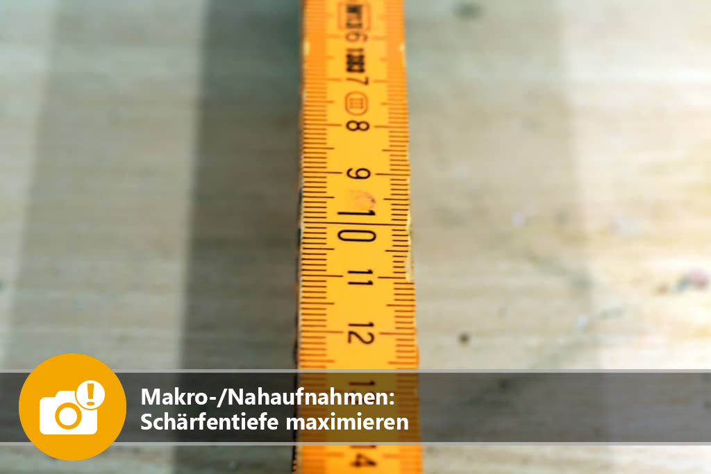
[13] K. Hirabayashi and T. Kurokawa, “Liquid crystal devices for optical communication and information processing systems,” Liq. Cryst., vol. 14, no. 2, pp. 307–317, 1993, https://doi.org/10.1080/02678299308027645.Search in Google Scholar
[89] J. Sun, E. Timurdogan, A. Yaacobi, E. S. Hosseini, and M. R. Watts, “Large-scale nanophotonic phased array,” Nature, vol. 493, no. 7431, pp. 195–199, 2013, https://doi.org/10.1038/nature11727.Search in Google Scholar PubMed


 Ms.Cici
 8618319014500