
Optical Universe Scientific - Your Choice Of Optical Instrument - scientific optics
Charge-coupleddevicediagram
Next we will connect the rails to the output of the regulator. This will allow us to later connect 5 volts to any part we would like.
Here we have connected the LEDs cathode to the negative side of the battery. All that's left is the resistor from the anode to the positive 5 volt rail to turn the LED on.
The main connections are complete. Now we'll add the filtering capacitors. Some capacitors are polarized and some are not. The 10 uF caps we are using are so we will need to be careful and place them in the circuit with the proper direction. The white stripe on our capacitors shows the negative side of the capacitors and needs to be connected to the negative parts of the circuit.
Charge coupled deviceworking principle
The most common CCD designs have a series of gate elements that subdivide each pixel into thirds by three potential wells oriented in a horizontal row. Each photodiode potential well is capable of holding a number of electrons that determines the upper limit of the dynamic range of the CCD. After being illuminated by incoming photons during a period termed integration, potential wells in the CCD photodiode array become filled with electrons produced in the depletion layer of the silicon substrate. Measurement of this stored charge is accomplished by a combination of serial and parallel transfers of the accumulated charge to a single output node at the edge of the chip. The speed of parallel charge transfer is usually sufficient to be accomplished during the period of charge integration for the next image.
Bestcharge coupled device detector
Let's start with the breadboard. A breadboard is a great little tool to help you prototype a circuit before ever having to make a PCB. It has pre-connected rows and columns which allow you to push electronic components into them to create your circuit. The next image shows which of the pins are usually connected together (not all breadboards are exactly the same!)
It’s pretty simple really; first, I want to explain what a power supply does, and then I will show you how to build one. We will start with a battery, and work our way up to a wall adapter. A power supply is responsible for providing a circuit with all the power it will need during normal operation. It provides the circuit with a certain voltage and current. The best way to think of this would be to imagine a hose with water running through it. The pressure of the water at the end of the hose is the voltage, and the amount of water going through the hose is the current. Most electronics need a certain amount of voltage and current to function.
By incorporating on-chip multiplication gain, the electron multiplying CCD achieves, in an all solid-state sensor, the single-photon detection sensitivity typical of intensified or electron-bombarded CCDs at much lower cost and without compromising the quantum efficiency and resolution characteristics of the conventional CCD structure.
The LED has an anode and cathode. The anode is connected to the + side and the cathode is connected to the - side. If the LED is placed in reverse, it will not turn on.
So now that we have that down, lets get to building! Here are all the parts we will use for this tutorial. In the picture you can see the LM7805 3 pin voltage regulator, two black 10 uF capacitors, two blue 0.1uf capacitors, one LED (clear lens with two legs), one 330 resistor (the part with the orange colored rings), and a breadboard (the white board with holes). Finally we have a 9 volt battery, and a connector. I have soldered some headers to the end, to make it easy to insert into a breadboard.
What we are going to do, is build this power supply, with a couple of simple changes. This regulator needs a 0.33 uF capacitor on the input side, and a 0.1 uF capacitor on the output side. The capacitors help filter the input and output from noise created by the power supply, and/or the load (i.e your project). We will add larger capacitors on both sides, to help keep our power supply clean, and noise free. Secondly, there is no way of knowing if our power supply is working, so we will add a little LED as our power indicator.
Michael W. Davidson - National High Magnetic Field Laboratory, 1800 East Paul Dirac Dr., The Florida State University, Tallahassee, Florida, 32310.
With the quick calculation above, you can see that for maximum brightness of our red LED, we need a resistor of 100 ohm. Since I don't really care about maximum brightness, I'd rather have a dimmer LED and save my battery; so I decided to use a 330 ohm resistor instead, which will still give me plenty of brightness and increase my battery life.
CCD vs CMOS
And here is the Multimeter reading the battery voltage. Be sure your multimeter is set to DC voltage mode and the red probe is connected to the correct terminal.
The next two pictures show both capacitors being added to the circuit. I had to trim the length of one of the pins for it to fit into the breadboard. Usually one pin is always longer than the other to show polarity. The input capacitors is on the top, and the output capacitors is on the bottom.
Next let's measure the output of our regulator. We will move the red jumper wire to the red rail which is connected to the output of the regulator.
And there you have it, it works! I know, you can hardly see the red LED... That's because of our camera flash, trust me, it's on and pretty bright. But wait a minute, just because the LED is on doesn't mean we are getting our desired 5 volts right? Well ya, it would be a wise decision to hook up a multi-meter and check the output before you connect anything to this supply. How do we do that? Let us start by checking the battery voltage.
Insides the breadboard are specially made metal bars and rails. When a component is placed on a breadboard, these bars hold the component in place and also allow you to electrically connect any other component to it using the same bar. Still not sure what to do with it? Lets start by placing the battery connector and regulator on the breadboard.
CCD camera
Next are two 0.1 uF capacitors (tiny blue ones in the picture). These are not polarized so we can put them anyway we would like.
Charge-coupleddevicePDF
Now it's time to add some wiring. We will use some of our pre-cut jumper wires to start making the circuit on breadboard. From the datasheet, we know that the pin on the far left of the regulator is the input, and the far right is the output. The middle is the 0 volts of our battery (we will call it ground for this tutorial). So to connect the input of the regulator to the battery, we will place a wire between pin 1 and 5, and one between 2 and 6.
After being collected in the potential wells, electrons are shifted in parallel, one row at a time, by a signal generated from the vertical shift register clock. The electrons are transferred across each photodiode in a multi-step process (ranging from two to four steps). This shift is accomplished by changing the potential of the holding well negative, while simultaneously increasing the bias of the next electrode to a positive value. The vertical shift register clock operates in cycles to change the voltages on alternate electrodes of the vertical gates in order to move the accumulated charge across the CCD. Figure 1 illustrates a photodiode potential well adjacent to a transfer gate positioned within a row of CCD gates.
The picture above is of our standard 5mm red LED. You can see in the picture that one leg of the LED is longer than the other. This is our anode and should be connected to the positive side of the power supply. The short pin is the cathode and should be connected to the negative side.
And there we have it. The regulator circuit is pretty much complete. Now let's add the power LED so we know when it's turned on.
The first part of any electronics project, is a power supply. Some projects use the USB port on your computer; others use a cheap wall adapter. Some are battery powered, and others are solar. With all these different options, how does one power their electronics project? Let us show you!
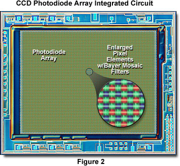
The principal architectural feature of a CCD is a vast array of serial shift registers constructed with a vertically stacked conductive layer of doped polysilicon separated from a silicon semiconductor substrate by an insulating thin film of silicon dioxide (see Figure 2). After electrons have been collected within each photodiode of the array, a voltage potential is applied to the polysilicon electrode layers (termed gates) to change the electrostatic potential of the underlying silicon. The silicon substrate positioned directly beneath the gate electrode then becomes a potential well capable of collecting locally-generated electrons created by the incident light. Neighboring gates help to confine electrons within the potential well by forming zones of higher potentials, termed barriers, surrounding the well. By modulating the voltage applied to polysilicon gates, they can be biased to either form a potential well or a barrier to the integrated charge collected by the photodiode.
Charge-coupleddeviceRadiology
When a ultraviolet, visible, or infrared photon strikes a silicon atom resting in or near a CCD photodiode, it will usually produce a free electron and a "hole" created by the temporary absence of the electron in the silicon crystalline lattice. The free electron is then collected in a potential well (located deep within the silicon in an area known as the depletion layer), while the hole is forced away from the well and eventually is displaced into the silicon substrate. Individual photodiodes are isolated electrically from their neighbors by a channel stop, which is formed by diffusing boron ions through a mask into the p-type silicon substrate.
For the sake of this tutorial, lets make that about 5 volts and let's save the current for later. For proper operation, we need to find a way to convert the voltage of our main supply (battery or wall adapter) down to 5 volts. This is where a regulator comes in. A regulator is a device that will convert the unregulated voltage to a stable 5 volts that we need to power our project. It's job is to maintain a steady 5 volts regardless of what the our battery is doing. The only caveat of a standard voltage regulator is that the main supply has to be slightly higher then what we want to achieve. So if we want 5 volts, we need at least 7 volts to maintain the steady 5 volts that we want. This power supply will not be able to convert from lower volts to 5. So once our battery is dead, our project will be too.
To measure voltage with a multimeter, you need to connect the multimeter in parallel with the circuit. So what we did above is added a pair of jumper wires to the breadboard. The red one is connected to pin 1 which is the same pin as our positive side of the battery. The second one is connected to our blue rail which is connected to the negative side of the battery. Now we can connect a multimeter set to voltage mode to our jumper wires and measure the voltage of the fresh 9 volt battery.
CCDs were invented in the late 1960's by research scientists at Bell Laboratories, who initially conceived the idea as a new type of memory circuit for computers. Later studies indicated that the device, because of its ability to transfer charge and the photoelectric interaction with light, would also be useful for other applications such as signal processing and imaging. Early hopes of a new memory device have all but disappeared, but the CCD is emerging as one of the leading candidates for an all-purpose electronic imaging detector, capable of replacing film in the emerging field of digital photomicrography.
CCDDetectorspectroscopy
There you go, our brand new 9 volt battery is providing our circuit with 9.37 volts! This would likely go down to being closer to 9.0 volts once we apply some real load on the circuit.
For a power light, we simply need to power the LED with the 5 volts being regulated by our circuit. Here we have to connect Pin 21 to 5 volts and Pin 22 to ground. Now we just need to add the LED and the resistor to protect the LED. LEDs do have a polarity.
After traversing the array of parallel shift register gates, the charge eventually reaches a specialized row of gates known as the serial shift register. Here, the packets of electrons representing each pixel are shifted horizontally in sequence, under the control of a horizontal shift register clock, toward an output amplifier and off the chip. The entire contents of the horizontal shift register are transferred to the output node prior to being loaded with the next row of charge packets from the parallel register. In the output amplifier, electron packets register the amount of charge produced by successive photodiodes from left to right in a single row starting with the first row and proceeding to the last. This produces an analog raster scan of the photo-generated charge from the entire two-dimensional array of photodiode sensor elements.
The second picture shows the output capacitors again, note the white stripe being connect to the ground line. I am using the blue rail as the negative side of my battery.
Here is our revised circuit; we have 4 capacitors instead of 2, and have added our power indicating red LED with a current limiting resistor, which is required for the LED, so it doesn't burn up. If your are wondering where the magic 330 ohm resistor value came from, it's a simple application of the V = IR equation. First we get the voltage drop and current requirements for our LED here. It has a voltage drop of about 3 volts, and draws 20 mA at maximum brightness.
We are getting 4.96 volts! This is well within the specs of our regulator, our circuit is working great. There you have it now we are ready to power our project with up to 750 mA of power!
Charge-coupled devices (CCDs) are silicon-based integrated circuits consisting of a dense matrix of photodiodes that operate by converting light energy in the form of photons into an electronic charge. Electrons generated by the interaction of photons with silicon atoms are stored in a potential well and can subsequently be transferred across the chip through registers and output to an amplifier. The schematic diagram illustrated in Figure 1 shows various components that comprise the anatomy of a typical CCD.
The regulator will happily power your project up to 750 mA but be careful. The metal tab of the regulator is meant to be connect to a heat sink. If you plan on using this circuit or any other voltage regulator circuit to its max current specs, be sure to use a heat sink and a fan to cool down the component. I hope you have enjoyed this lesson. Let us know if you have any questions on our forum or you can get in touch with us using the contact us page.
Fabricated on silicon wafers much like integrated circuits, CCDs are processed in a series of complex photolithographic steps that involve etching, ion implantation, thin film deposition, metallization, and passivation to define various functions within the device. The silicon substrate is electrically doped to form p-type silicon, a material in which the main carriers are positively charged electron holes. Multiple dies, each capable of yielding a working device, are fabricated on each wafer before being cut with a diamond saw, tested, and packaged into a ceramic or polymer casing with a glass or quartz window through which light can pass to illuminate the photodiode array on the CCD surface. Explore the sequence of steps necessary to build a CCD using our interactive Java tutorial, which is linked from the dialog box.


 Ms.Cici
 8618319014500