
Optical Glass Ball Lenses and Half ball lenses - fused silica ball lens
Depending on the type of the photodiode, load resistance can affect the response speed. For maximum bandwidth, we recommend using a 50 Ω coaxial cable with a 50 Ω terminating resistor at the opposite end of the cable. This will minimize ringing by matching the cable with its characteristic impedance. If bandwidth is not important, you may increase the amount of voltage for a given light level by increasing RLOAD. In an unmatched termination, the length of the coaxial cable can have a profound impact on the response, so it is recommended to keep the cable as short as possible.
Thermistors were used to monitor the temperatures of each photodiode continuously during the experiment. A piece of thermal tape was used to hold the thermistor flush against the TO cans of the FDG50, FGAP71, and the FGA10 during testing. The photosensor of the FDS1010 is mounted on a ceramic substrate, and when it was tested the thermistor was taped to the back of the substrate. The electrical connection between the thermistor and TSP01 temperature logger was performed using BNC cables, BNC-to-BNC bulkhead feedthroughs to route the signal out of the nested boxes, and a custom BNC-to-phono jack cable to connect to the temperature logger.
Experimental SetupThe experimental setup was designed to ensure a constant reverse-bias voltage across the photodiode, control the temperature of the detector, block light from reaching the detector, and establish an electrical path between the detector and the Keithley 6487 ammeter that isolated the measured current from extraneous electromagnetic interference (EMI) noise sources. Dark currents for these detectors can be on the order of nA, which made it important to control these conditions to ensure accurate measurements.
For our experiment, we used the SM1PD1A mounted photodiode, which consists of an FDS1010 photodiode in an SM1-threaded housing. An 830 nm superluminescent diode was used as the light source. A beamsplitter directed 20% of the light to a monitor photodiode while the remainder was transmitted through a focusing lens. Power values were calibrated using an integrating sphere, while the beam size of the focusing beam was calibrated with a beam profiler mounted to a translation stage. After calibration, the beam profiler was replaced with the device under test (DUT), an SM1PD1A at a 0 V bias. The output current was measured with an ammeter to remove the need for a load resistor. We then recorded datasets as the beam diameter was continuously scanned from 0.06 mm to 5 mm while power was held constant, as well as measurements for beam diameters ranging from 1 mm to 5 mm (measured to the 5% clip level) as the incident power was continuously scanned from 0.12 mW to 5 mW.
where is is the shot noise, Id is the dark current, q is the electron charge, and fBW is the bandwidth, which will be set to 1 Hz to allow for comparison between different photodiodes.
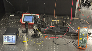
Experiment An experiment was developed to measure the change in VL with respect to changes in P. Output from a fiber-coupled laser diode was collimated, passed through a neutral density filter, and then focused onto the Device Under Test (DUT) via an off-axis parabolic mirror. A photograph of the setup used can be seen in Figure 1 to the upper right. Neutral density filters with a range of optical densities were used to vary the power incident on the photodiode. For each photodiode used, the distance between the sensor surface and focusing mirror was adjusted so that the spot size was approximately half the size of each photodiodes’ detector area. An oscilloscope was used to measure V0, VL, and the sum Veff + VL. A multimeter was used to measure the effective bias directly.
Response May Vary as Different Regions of the Photodiode's Active Area are Illuminated1,2An electron that has escaped the bonds of its host atom by absorbing the energy of a photon is a photo-generated electron. A photo-generated electron contributes to the photocurrent only if the electron is able to successfully travel from where it was generated, across the semiconductor material, and to an electrical contact. A photo-generated electron does not contribute to the photocurrent if it is re-absorbed by the semiconductor material before reaching a contact, which is a more likely outcome if the electron encounters a defect.
We present laboratory measurements showing the effect of beam size on the saturation point of a Thorlabs silicon photodiode. As defined here, saturation is a 1% deviation from the linear response region. As illustrated in Figure 1, the photodiode saturated at lower incident power levels as the beam size decreased. Several additional calculations and experiments were performed to verify the cause of the change in saturation was not a function of the power density. These results suggest that users should be cognizant of the beam size when attempting to measure absolute power with a power sensor, such as our S130C photodiode power sensor.
The detector will exhibit lower responsivity at lower chopping frequencies. Frequency response and detectivity are maximized for
SummaryThis tab contains a collection of experiments performed at Thorlabs regarding the performance of photodiodes we offer. Each section is its own independent experiment, which can be viewed by clicking in the appropriate box below. Photodiode Saturation Limit and Noise Floor explores how different conditions, including temperature, resistivity, reverse-bias voltage, responsivity, and system bandwidth, can affect noise in a photodiode's output. Photodiode Spatial Uniformity explores variations in the responsivity as a small-diameter light beam is scanned across the active area of the photodiode. Photodiodes with different material compositions are tested, and eight units of one silicon-based model are tested to investigate unit-to-unit variations. Dark Current as a Function of Temperature and Noise Equivalent Power (NEP) as a Function of Temperature describe how dark current and NEP, respectively, vary with temperature and how measurements are affected. Beam Size and Photodiode Saturation shows how the photodiode saturation point changes with the incident beam size and investigates several models to explain the results. Bias Voltage examines the effects of incident power on the effective reverse bias voltage of a photodiode circuit and verifies a reliable model for predicting those changes.
One can also use a photodetector with an amplifier for the purpose of achieving high gain. The user can choose whether to operate in Photovoltaic of Photoconductive modes. There are a few benefits of choosing this active circuit:
Electrons generated near defects are more likely to be re-absorbed and less likely to contribute to the photocurrent. While the density of defects in a semiconductor can be minimized, the semiconductor crystals used in photodiodes are not perfect. It is also not unusual for the density of defects to vary throughout the volume of the semiconductor crystal, as well as for the growth of some semiconductor materials to be more prone to forming defects than others.
During the scan, the position of the beam remained stationary, and the two LNR50S motorized stages were used to translate the photodetector in the two directions perpendicular to the optic axis. To ensure that the entire active area of the photodetector was tested, the dimensions of the scan area exceeded the dimensions of the active area.
The DET series detectors are modeled with the circuit depicted above. The detector is reverse biased to produce a linear response to the applied input light. The amount of photocurrent generated is based upon the incident light and wavelength and can be viewed on an oscilloscope by attaching a load resistance on the output. The function of the RC filter is to filter any high-frequency noise from the input supply that may contribute to a noisy output.
ISO 11146 is intended to provide a simple, consistent way of describing the width of a beam. This notebook summarizes the mathematical definitions. [1]:. import ...
Your cart will be set to In-Store Pickup By adding this item to your cart, the shipping option will not be available for your order. The In-Store Pickup option will now be defaulted at checkout.
Photodiodeworking principle
These span approximately 6 orders of magnitude. In all cases, the dark current increased with the temperature of the photodiode, as expected. The individual points on this graph, plotted as diamonds, are the values of the dark current specified for each detector at 25 °C. These points specify a maximum value of dark current at 25 °C; each diode's dark current must be equal to or less than this value at 25 °C, but the dark current may exceed this specification at higher temperatures, as is the case for all but the measured FDS1010 detector.
To complement our photodiode product line, we offer mounted photodiodes and a range of compatible photodiode sockets. Please note that the PDs sold below are not calibrated, meaning responsivity will differ slightly from lot to lot; refer to the Response Variation tab for more information. We also offer calibrated photodiodes, which come with with NIST-traceable calibration, to correct for the differences in responsivity. Many of our photodiodes can be reverse voltage biased using the PBM42 DC Bias Module for faster speed and higher optical power detection.
Thermal, or Johnson, noise is due to the random thermal motion of the charge carriers. Thermal noise will be generated only by the resistive elements of the system. For the photodiode detector, the shunt resistance needs to be considered. Shunt resistance is the resistance of the zero-biased photodiode p-n junction; put another way, it is the inverse of the slope of the I-V curve at the zero-voltage point. Since it is difficult to correctly calculate the slope at the zero crossing, the generally accepted industry practice is to measure the current at V = ±10 mV and then calculate the slope. Then the thermal noise due to the shunt resistance, RSH, can be expressed as:
Photodiodecircuit
Results (Click More [+] to Expand the Following Tables, and Click Less [-] to Hide Them)The measurement data were normalized and then plotted with respect to the measurement position. The data in each measurement set were normalized with respect to the value at the center of the active area, which resulted in plots that show the variation of the responsivity across each photodetector's active area and allow the results from these nine different photodetector models to be compared. The plotted data were also processed to remove data points with values indistinguishable from noise. This was done to eliminate data points corresponding to measurements made outside of the active area of each photodetector. However, this approach also removed some measurements made within, but close to, the outer edges of the active areas. The lower photocurrent generated by these regions may have been due to the beam spot partially illuminating regions outside of the active area, as well as photocurrent suppressed by a higher density of defects near the edges.
Series ResistanceSeries resistance is the resistance of the semiconductor material, and this low resistance can generally be ignored. The series resistance arises from the contacts and the wire bonds of the photodiode and is used to mainly determine the linearity of the photodiode under zero bias conditions.
The photoconductor signal will remain constant up to the time constant response limit. Many detectors, including PbS, PbSe, HgCdTe (MCT), and InAsSb, have a typical 1/f noise spectrum (i.e., the noise decreases as chopping frequency increases), which has a profound impact on the time constant at lower frequencies.
The responsivity of a particular photodiode varies from lot to lot. Due to this, the photodiode you receive may have a slightly different response than what is represented below. For example, to the right, a graph for the FDS1010 photodiode shows the extent that the response may vary. This data was collected from 104 photodiodes. Minimum, Average, and Maximum responsivity was calculated at each data point and has been plotted.
For our experiment we used the FDS100 Si Photodiode as the photodiode under investigation. The collimated output of a fiber-pigtailed laser diode was used as the light source with output power from 0 to 50 mW. The collimated beam was incident upon a beamsplitter that transmitted the majority of the light to the photodiode under investigation and reflected the rest towards a reference power sensor. The photodiode response was then evaluated under various resistive loads and with different reverse bias voltages.
PhotoconductiveIn photoconductive mode, an external reverse bias is applied, which is the basis for our DET series detectors. The current measured through the circuit indicates illumination of the device; the measured output current is linearly proportional to the input optical power. Applying a reverse bias increases the width of the depletion junction producing an increased responsivity with a decrease in junction capacitance and produces a very linear response. Operating under these conditions does tend to produce a larger dark current, but this can be limited based upon the photodiode material. (Note: Our DET detectors are reverse biased and cannot be operated under a forward bias.)
Pulsed laser radiation parameters are illustrated in Figure 1 and described in the table. For quick reference, a list of equations is provided below. The document available for download provides this information, as well as an introduction to pulsed laser emission, an overview of relationships among the different parameters, and guidance for applying the calculations.
Since these photodetectors represent a small sample size, these measurements are representative of the other photodetectors of its model, but results obtained using other units of the same model may vary. The measurements acquired for these photodetector units were repeatable, but no two semiconductor crystals are identical and unit-to-unit variations should be expected. The following tables show that:
The data curves plotted in Figure 6 show that the calculated NEP magnitudes differed depending on the material composing the photodiode. From lowest to highest:
Introduction The bandwidth (and rise time) of a photodiode is known to be a function of the effective bias across it. Therefore, the effective bias must be tuned in response to the generated photocurrent from the optical power incident on the diode to maintain the desired bandwidth. This lab fact investigates the relationship between the effective reverse bias voltage across a photodiode and the CW optical power incident on it in order to create a reliable model of a biased photodiode.
NEP was determined over 25 to 55 °C for four representative unpackaged photodiodes: the Si-based FDS1010, the Ge-based FDG50, the GaP-based FGAP71 (previous generation), and the InGaAs-based FGA10.
Fibre Channel D-Sub connectors offer high Data rate 6.25 Gbps, high shock and data resistance and high density quadrax. The main function associated with ...
The detector enclosure consisted of a pair of nested aluminum metal boxes, which are shown with their covers off in Figure 1. Only one box would be required to create a light-tight environment for the photodiode, but an outer box was included in the setup to shield the inner box from EMI. The detector was placed inside the inner box, and it was electrically connected to the Keithley 6487 ammeter. The ammeter provided the required reverse-bias voltage and received the output current signal. The electrical signals between the ammeter and the photodiode were routed through the two boxes using a combination of cables and feedthroughs. The bias voltage was connected to the photodiode using coax cables and BNC-to-BNC feedthroughs in the walls of both metal boxes. The current signal from the photodiode was connected to the BNC end of a BNC-to-Triax feedthrough integrated into the wall of the inner box. The signal was then routed through the outer box and to the Keithley 6487 using triax cables and a Triax-to-Triax feedthrough in the outer box. Triax cables were used because coax cables are poorly shielded, and using a coax cable to route the signal to the ammeter could introduce noise from EMI sources to the signal read from the detector. As the outer box shields the inner box from EMI, the noise introduced on the signal as it travels from the detector to the BNC-to-Triax feedthrough is mitigated.
Photodiodesensor
I use a version of number 1 because I ware glasses and #1 works with glasses. I set it up for maximum magnification and never change it. Once in a while I use ...
Dark current is a relatively small electric current present in photosensitive devices that flows through the device, including when there is no incident light. More information on the dark current can be found in the "Dark Current as a Function of Temperature" section above. Shot noise is due to the quantized nature of the charge carriers. For the case where there is no light incident on the detector, it can be calculated from the dark current of the detector using the equation [2]
Figure 6 shows the calculated NEP vs. temperature for each diode. Since the NEP is a function of responsivity, which varies with wavelength, the NEP values are calculated at the peak responsivity value as given in the table to the right.
The upper wavelength of a photodetector's responsivity is limited by inherent properties of the semiconductor material. In order for an incident photon to contribute to the photocurrent, the photon must have enough energy to free an electron from its bonds to its host atom. Photons with wavelengths above the upper wavelength limit do not have enough energy. The semiconductor material composing the photodiode determines the wavelength of this limit.
Experimental Setup The experimental setup was designed to ensure a constant reverse-bias voltage across the photodiode, control the temperature of the detector, block light from reaching the detector, and establish an electrical path between the detector and the Keithley 6487 ammeter that isolated the measured current from extraneous electromagnetic interference (EMI) noise sources. Dark currents for these detectors can be on the order of nA, which made it important to control these conditions to ensure accurate measurements.
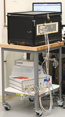
A custom temperature chamber based on a XE25C9 standard enclosure was used to conduct these tests. It is shown on top of the cart in Figure 3. The enclosure had a floor and four walls, and insulation was attached to all inner and outer surfaces. A lid for the enclosure was fashioned from a sheet of hardboard bordered with XE25 rails, and insulation was attached to the inner surface of the hardboard. Six resistive foil heaters were affixed to the walls of the XE25C9 enclosure, and they were driven using the PRO8000 chassis fitted with six TED8040 thermoelectric cooler (TEC) controller cards placed on the bottom shelf of the cart in Figure 2. Each TED8040 was interfaced with a heater and a thermistor installed in the chamber. The reading from the thermistor determined the current sent to drive the heater. The chamber was not actively cooled; cooling was instead performed by withdrawing the current driving the heaters and, as an option, opening the lid of the chamber.
ResponsivityThe responsivity of a photodiode can be defined as a ratio of generated photocurrent (IPD) to the incident light power (P) at a given wavelength:
Determining whether emission from a pulsed laser is compatible with a device or application can require referencing parameters that are not supplied by the laser's manufacturer. When this is the case, the necessary parameters can typically be calculated from the available information. Calculating peak pulse power, average power, pulse energy, and related parameters can be necessary to achieve desired outcomes including:
[1] G. P. Agrawal, Fiber-Optic Communication Systems, 2nd ed., John Wiley & Sons, Inc., New York, 1997. (Particularly Chapter 4) [2] A. Rogalski, K. Adamiec, and J. Rutkowski, Narrow-Gap Semiconductor Photodiodes, SPIE Press, Bellingham, WA, 2000.
Fits RX 350L (2018 - 2022)Wheel Alignment AdjustIf you’ve just purchased new tires, protect your investment with a wheel alignment. If your Lexus RX 350L pulls to the left or right, your steering wheel is off-center, or you’ve noticed uneven tread wear on your tires, a Lexus technician can align the steering and suspension system.
Highest resolution target available on the commercial market; Conforms to 1951 US Air Force MIL-STD-150A; Minimum feature size of 137 nanometer bar width; High ...
Note that this result is the total noise expressed for the current output of the photodiode, while the NEP is expressed in terms of incident optical power. Thus, to compare with the NEP specifications a typical responsivity value,, is chosen for the specified wavelength:
Assuming that the voltage drop across the load resistor (VL) is linear with respect to increasing P, the ratio of the change in VL and P can be established as the ratio:
Photodiodeapplication
Jedes digitale Foto einer Kamera hat zunächst die exakt gleiche Pixelgröße, also beispielsweise 6000 x 4000 Pixel, oder ca. 24 Megapixel, und bezieht sich auf ...
It is necessary to be able to correctly determine the level of the output current to expect and the responsivity based upon the incident light. Depicted in Figure 1 is a junction photodiode model with basic discrete components to help visualize the main characteristics and gain a better understanding of the operation of Thorlabs' photodiodes.
For convenience, both dark current and photocurrent are discussed as being independent of voltage over a range of voltages when the photodiode is reverse biased; however, the current flowing in real-world reverse-biased photodetectors is not completely independent of voltage over any voltage range. Regardless of whether the diode is illuminated, the current will increase as the magnitude of the reverse-bias voltage increases. In addition, if the reverse-bias voltage is increased beyond a certain threshold, the photodiode will suffer reverse breakdown, in which the magnitude of the current increases exponentially and permanent damage to the diode is likely.
To find how Veff changes with respect to the incident optical power (P), iPD is replaced in the above equation with its definition as the product of the wavelength-dependent responsivity [ℜ(λ)] of the photodiode and P:
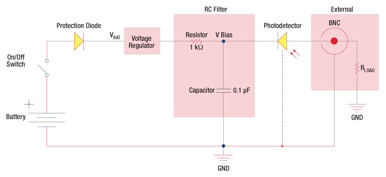
Figure 1: Parameters used to describe pulsed laser emission are indicated in the plot (above) and described in the table (below). Pulse energy (E) is the shaded area under the pulse curve. Pulse energy is, equivalently, the area of the diagonally hashed region.
The plots to the right and below summarize the measured results for the various tested configurations. From these graphs the changes to the photodiode's linear response, noise floor, and saturation limit can be observed under different reverse voltage biases and load resistances. Figure 1 provides an overview of the photodiode response with a reverse voltage bias of 5 V and resistive load of 10 kΩ. The photodiode saturated at the upper limit of the response when the output photovoltage approached the reverse bias voltage. The noise floor at the lower limit of the response was a result of dark current and the thermal noise from the resistive load (Johnson noise). Figure 2 summarizes the results obtained using the photodiode with a 1 kΩ resistive load and various reverse bias voltages. It illustrates that the saturation limit can be raised by increasing the reverse bias voltage (within specification). Figure 3 summarizes the results from using the photodiode with a 5 V reverse bias voltage and various resistive loads. It illustrates that the slope of the photovoltage response increased as the load resistance was increased. Figure 4 summarizes the noise floor results obtained using a 0 V reverse bias voltage and various resistive loads. The noise floor increased when larger load resistances were used. It is important to note that the 1 kΩ data was measured above the theoretical Johnson noise due to the voltage noise within the measurement system. Minimal change in the overall noise floor was seen when using a 5 V reverse bias voltage. For details on the experimental setup employed and these summarized results, please click here.
Junction CapacitanceJunction capacitance (Cj) is an important property of a photodiode as this can have a profound impact on the photodiode's bandwidth and response. It should be noted that larger diode areas encompass a greater junction volume with increased charge capacity. In a reverse bias application, the depletion width of the junction is increased, thus effectively reducing the junction capacitance and increasing the response speed.
The effective bias voltage (Veff) across the photodiode equals the initial voltage from the source (V0) minus the product of the photocurrent (iPD) and the sum of the resistance of the bias module's resistor (RP) and the load resistor (RL).
PINphotodiode
where it is the thermal noise (expressed as a current), kB is Boltzmann's constant, T is temperature, RSH is shunt resistance, and fBW is the bandwidth.
When a photodiode is illuminated, the current generated by the incident light adds to the dark current. The carriers in the photocurrent are generated by the energy contained in the photons of the incident light. Above a certain illumination threshold intensity, the magnitude of the photocurrent exceeds the magnitude of the dark current. When the photocurrent is larger than the dark current, the magnitude of the photocurrent can be calculated by measuring the total current and then subtracting the contribution of the dark current. When the photocurrent is smaller than the dark current, the photocurrent is undetectable. Because of this, it is desirable to minimize the levels of dark current in photodiodes.
By continuing to use this website, you agree to our use of cookies to give you the best shopping experience. Terms and Conditions of Sale
ProcedureThe diameter of the beam was scaled according to the active area of the photodetector, so that approximately 3600 measurements were taken in a 60 x 60 grid across the surface of each photodiode. The beam diameter used for each photodiode was between 50 µm and 500 µm, and the size used to make a particular measurement is included in the notes that accompany each plot in the following expandable tables. To view this information, click on the plot of interest.
Noise Equivalent Power (NEP) was determined as a function of temperature for several unmounted photodetectors. As is described in the following section, NEP is a common metric used to describe the minimum sensitivity of a photodetector. Measurements were taken for silicon (Si), germanium (Ge), gallium phosphide (GaP), and indium gallium arsenide (InGaAs) reverse-biased photodiodes over temperatures from 25 °C to approximately 55 °C.
The dark current present is also affected by the photodiode material and the size of the active area. Silicon devices generally produce low dark current compared to germanium devices which have high dark currents. The table below lists several photodiode materials and their relative dark currents, speeds, sensitivity, and costs.
For dark current measurements, the bias voltage was set to 5 V. In order to calculate the shunt resistance, measurements of the current were made with the bias voltage set to +10 mV and -10 mV.
The output signal strength from a photodetector is significantly affected by the optical power and wavelength of the incident light. A measure of this relationship is responsivity, which is the magnitude of the output photocurrent divided by the optical power of the incident light. While responsivity has units of ampere per watt, it also varies with wavelength. Often overlooked is that responsivity can also vary as different regions of the photodiode's active area are illuminated.
For information on the photodiode saturation limit and the noise floor, as well as a collection of Thorlabs-conducted experiments regarding spatial uniformity (or varying responsivity) and dark current as a function of temperature, refer to the Lab Facts tab. This tab also outlines the theory and methods we use to define the specifications of our photodiodes. For example, the Noise Equivalent Power (NEP) as a Function of Temperature section provides background on NEP values specified by shot noise and thermal noise. With zero bias (Photovoltaic Mode), the NEP is specified by the thermal noise only, which is caused by the shunt resistance of the photodiode. The Photodiode Tutorial provides more general information regarding the operation, terminology, and theory of photodiodes.
Noise Equivalent PowerThe noise equivalent power (NEP) is the input signal power that results in a signal-to-noise ratio (SNR) of 1 in a 1 Hz output bandwidth. This is useful, as the NEP determines the ability of the detector to detect low level light. In general, the NEP increases with the active area of the detector and is given by the following equation:
Modes of Operation (Photoconductive vs. Photovoltaic)A photodiode can be operated in one of two modes: photoconductive (reverse bias) or photovoltaic (zero-bias). Mode selection depends upon the application's speed requirements and the amount of tolerable dark current (leakage current).
Experimental ResultsThe data curves plotted in Figure 4 are the dark currents measured for the Si-based FDS1010, the Ge-based FDG50, the GaP-based FGAP71, and the InGaAs-based FGA10. Figure 5 shows the calculated shunt resistance values for the same diodes as Figure 4. Data were acquired continuously while the temperature was between 25 °C and 55 °C (shaded region of Figure 7). Figure 7 is representative of the temperature measured at the photodiode during the experiment. The temperature profile included an initial segment of increasing temperature, followed by a soak that allowed the photodiode to reach the maximum temperature, and concluded with a cool-down. The data plotted in Figures 4 and 5 include all dark current measurements measured between approximately 25 °C and 55 °C; current measurements taken at the same temperature, but at different times, overlay one another for each diode.
Inhomogeneity on the edge of an active area of the detector can generate unwanted capacitance and resistance that distorts the time-domain response of a photodiode. Thorlabs therefore recommends that the incident light on the photodiode is well centered on the active area. This can be accomplished by placing a focusing lens or pinhole in front of the detector element.
A custom temperature chamber based on a XE25C9 standard enclosure was used to conduct these tests. It is shown on top of the cart in Figure 3. The enclosure had a floor and four walls, and insulation was attached to all inner and outer surfaces. A lid for the enclosure was fashioned from a sheet of hardboard bordered with XE25 rails, and insulation was attached to the inner surface of the hardboard. Six resistive foil heaters were affixed to the walls of the XE25C9 enclosure, and they were driven using the PRO8000 fitted with six TED8040 thermoelectric cooler (TEC) controller cards placed on the bottom shelf of the cart in Figure 3. Each TED8040 was interfaced with a heater and a thermistor installed in the chamber. The reading from the thermistor determined the current sent to drive the heater. The chamber was not actively cooled; cooling was instead performed by withdrawing the current driving the heaters and, as an option, opening the lid of the chamber.
Since the results presented in Figure 3 coupled the beam size change with a change in optical power density, we performed another experiment to increase the power density incident on the sensor within the same envelope of beam area to see if there was a change in the saturation point. This was done by segmenting the Gaussian beam into an array of beamlets with a microlens array, concentrating the overall optical power into smaller spots within the same Gaussian envelope. This created larger power densities while maintaining a similar electrical path to the sensor leads. Figure 4 shows the same results as Figure 2 with the results from the microlens array overlaid as dashed lines. Since the results are nearly identical to the original Gaussian beam for all diameters, the saturation appears to be dependent on the overall beam diameter and independent of the power density. In the complete Lab Facts presentation, we discuss how these results support the theory of Scholze et al. that the change in saturation with beam size is due to a change in the series resistance of the photodiode [1].
The figures show the results from the measurements. Figure 1 (right) and Figure 2 (below) show the deviation from linear response for continuously varying beam diameter at a fixed 1 mW incident power (Figure 1) and continuously varying incident power for several beam diameters (Figure 2). Figure 1 shows that for a 1 mW input, the photodiode saturated at beam sizes less than 300 µm. Figure 2 shows that beam diameters ≥2 mm did not saturate at the power levels investigated.
We are a leading measurement, inspection and remediation company working within the energy sector with over 20 years' experience developing innovative solutions ...
PhotovoltaicIn photovoltaic mode the photodiode is zero biased. The flow of current out of the device is restricted and a voltage builds up. This mode of operation exploits the photovoltaic effect, which is the basis for solar cells. The amount of dark current is kept at a minimum when operating in photovoltaic mode.
D Wueller · 6 — An ISO 21550 Standard to measure the ability of scanners to reproduce tones especially in the dark areas of the original is currently under development (in ...
Measurement ObjectivesSeveral photodetectors were tested to investigate the uniformity of the responsivity across their active areas. The spatially dependent responsivities of one GaP-based, four Si-based, two InGaAs-based, and two Ge-based photodetectors were measured at selected wavelengths. Testing was conducted to investigate the spatial uniformity of the responsivity of:
Responsivity is Wavelength Dependent1,2One reason responsivity varies with respect to wavelength is the relationship among optical power, wavelength, and photo-generated electrons. A light beam illuminating a surface provides an optical power equal to the energy in the beam divided by the time the surface was illuminated. The energy in a single-wavelength beam equals the number of incident photons times the energy of a single photon. Decreasing the wavelength of the light increases the energy of the photons. If the wavelength is decreased, but the optical power is kept the same, there are fewer incident photons. A single photon can generate no more than a single electron of photocurrent in these photodetectors. Due to this, reducing the wavelength of the incident light while holding its optical power constant results in a reduced photocurrent. Since responsivity relates the output photocurrent to the incident optical power, instead of to the number of incident photons per unit time, responsivity is lower at lower wavelengths. The responsivity curves plotted in Figure 1 are examples showing responsivity increasing with wavelength.
The characteristic current-voltage relationship of p-n junction photodiodes, as diagrammed in Figure 1, possesses forward-biased and reverse-biased voltage regimes. In the reverse-biased voltage regime, in which p-n junction photodiodes are operated, a potential difference applied across the diode resists the flow of current. Ideally, if no light is incident on a reverse-biased photodiode, no current flows.
Photodiodediagram
Experimental Setup (Components Labeled in Figure 2 are Labeled in the Following)The experimental setup consisted of a light source (not shown) that was fiber-coupled to an RC12APC-P01 collimator (A), which was installed in a KM100T kinematic mount. An AC254-150-A achromatic doublet lens with a 150 mm focal length (B), which was installed in a ST1XY-D mount, focused the light on the active area of the photodetector (D), which was mounted with the help of a KB1P magnetic quick-release carriage set. Other components in the vertical arm included a previous-generation LTS150 motorized linear translation stage (C), an XT66P1 vertical mounting plate, an XT66-500 66 mm construction rail, and four XT66C4 clamping platforms. The components in the horizontal arm included two previous-generation LNR50S motorized linear translation stages (E), an LNR50P3 XY adapter plate, a baseplate, and two BSC201 closed-loop stepper motor controllers (not shown), which scanned the beam across the active area of the photodetector (D). Most light sources were products from our Superluminescent Diode series. The exception was the 405 nm light source, which was an S3FC405 benchtop laser source.
Thorlabs stocks a wide selection of photodiodes (PD) with various active area sizes and packages. Discrete PIN junction photodiodes include silicon (Si) and indium gallium arsenide (InGaAs) materials. Germanium (Ge) photodiodes, which are based on an N-on-P structure, are also available.
Is it safe to use a detector with a specified maximum peak optical input power of 75 mW to measure the following pulsed laser emission?
Thermistors were used to monitor the temperatures of each photodiode continuously during the experiment. A piece of thermal tape was used to hold the thermistor flush against the TO cans of the FDG50, FGAP71, and the FGA10 during testing. The photosensor of the FDS1010 is mounted on a ceramic substrate, and when it was tested the thermistor was taped to the back of the substrate. The electrical connection between the thermistor and TSP01 temperature logger was performed using BNC cables, BNC-to-BNC bulkhead feedthroughs to route the signal out of the nested boxes, and a custom BNC-to-phono jack cable to connect to the temperature logger.
Shunt ResistanceShunt resistance represents the resistance of the zero-biased photodiode junction. An ideal photodiode will have an infinite shunt resistance, but actual values may range from the order of ten Ω to thousands of MΩ and is dependent on the photodiode material. For example, and InGaAs detector has a shunt resistance on the order of 10 MΩ while a Ge detector is in the kΩ range. This can significantly impact the noise current on the photodiode. For most applications, however, the high resistance produces little effect and can be ignored.
Results VL was plotted against P for each DUT; an example of the results for the silicon photodiode can be seen in Figure 3 to the right. A linear trend line was created for each data set, and the slope of that line corresponds to m in Equation 4. This value can be used in Equation 5 to calculate the effective bias voltage. Then, Veff can be plotted with respect to the incident power and compared to the measured values from the oscilloscope. These results are shown in the three graphs displayed in Figure 4 below. The model was found to be consistent with measured experimental results, which showed that Veff decreases as P increases (with V0, RP, and RL held constant). This effect is significant, because the voltage set at the voltage source is not necessarily the bias voltage applied to the photodiode; one must account for resistive components within the circuit to calculate the effective bias voltage applied across the photodiode.
Photodiodecharacteristics
Perform with confidence, knowing you have everything in place to support the most popular ambulatory surgical procedures. Our surgical solutions can help you ...
Experimental Limitations Measurements were performed using a single representative of each detector type, as these data were intended to illustrate overall trends. These data should not be taken as specific for a particular diode. The measured dark current is a function of voltage bias, temperature dependence of resistive loads, and other effects. Efforts were made to suppress their influence on these measurements, including using the Keithley 6487 ammeter to provide the required 5 V reverse bias. Using the ammeter removed the need to use a load resisitor, which may exhibit its own temperature dependence. The thermistor was placed as close to the semiconductor sensor as was possible, but it was not placed in direct contact with the sensor. Because of this, there may have been a difference between the measured temperature and the temperature of the semiconductor material. The dark current was measured while the temperature of the environmental chamber was continuously varied. Humidity was not controlled during this experiment.
Photodiodesymbol
The TED8040 units are designed to be interfaced with TECs, which produce heat when current flows in one direction, and which provide cooling when the current flows in the opposite direction. Because of this, when the enclosure exceeded the setpoint temperature, the TED8040 units in this experimental setup did not cut off the driving current. They instead reversed the current flow in an effort to produce cooling. In contrast to TECs, resistive foil heaters generate heat regardless of the direction of current flowing through them. In order to divert the driving current from the heaters, an electrical circuit, diagrammed in Figure 4, that included two rectifying diodes was designed and implemented. Rectifying diodes allow current to flow only in one direction. When the temperature reading from the thermistor was lower than the setpoint temperature, current flowed in the direction of the red arrows and through the resistive heater, and heat was generated. When the temperature of the enclosure exceeded the setpoint temperature, the TED8040 controllers reversed the direction of the current, so that it flowed in the direction of the blue arrows. Under this condition, the circuit diverted the current from the heaters and the chamber was allowed to cool.
Thorlabs offers spectral-flattening filters that are designed to improve the response uniformity of our silicon photodiodes. Click here to learn more.
Dark currents were measured over temperatures of 25 °C to approximately 55 °C for four representative unpackaged photodiodes: the Si-based FDS1010, the Ge-based FDG50, the GaP-based FGAP71 (previous generation), and the InGaAs-based FGA10.
Under real-world conditions, random processes in the semiconductor material of the photodiode always generates current carriers (electrons and holes) that produce current. These current generation processes are not driven by the photogeneration of electrons and holes. Instead, they are largely driven by the thermal energy contained in the semiconductor material.[1] This dark current is generally small, but it is present when the photodiode is reverse biased and not illuminated. Dark current magnitudes vary for photodiodes of different material compositions; the efficiencies of the thermal generation processes depend on the type and crystal quality of the semiconductor used in the detector's sensing head. The magnitude of the dark current can be expected to increase as the temperature of the photodiode increases.
Here, S/N is the Signal to Noise Ratio, Δf is the Noise Bandwidth, and Incident Energy has units of W/cm2. For more information on NEP, please see Thorlabs' Noise Equivalent Power White Paper.
Experimental Results The data curves plotted in Figure 5 are the dark currents measured for the Si-based FDS1010, the Ge-based FDG50, the GaP-based FGAP71, and the InGaAs-based FGA10. Data were acquired continuously while the temperature was between 25 °C and 55 °C (shaded region of Figure 6). Figure 6 is representative of the temperature measured at the photodiode during the experiment. The temperature profile included an initial segment of increasing temperature, followed by a soak that allowed the photodiode to reach the maximum temperature, and concluded with a cool-down. The data plotted in Figure 5 include all dark current measurements measured between 25 °C and 55 °C; current measurements taken at the same temperature, but at different times, overlay one another for each diode.
Circuit Analysis To begin creating this model, the photodiode circuit shown in Figure 2 to the right is examined using Ohm’s law and assuming a constant DC voltage source; this yields the equation
It is not safe to use the detector to measure this pulsed laser emission, since the peak power of the pulses is >5 orders of magnitude higher than the detector's maximum peak optical input power.
The detector enclosure consisted of a pair of nested aluminum metal boxes, which are shown with their covers off in Figure 2. Only one box would be required to create a light-tight environment for the photodiode, but an outer box was included in the setup to shield the inner box from EMI. The detector was placed inside the inner box, and it was electrically connected to the Keithley 6487 ammeter. The ammeter provided the required 5 V reverse-bias and received the output current signal. The electrical signals between the ammeter and the photodiode were routed through the two boxes using a combination of cables and feedthroughs. The 5 V bias voltage was connected to the photodiode using coax cables and BNC-to-BNC feedthroughs in the walls of both metal boxes. The current signal from the photodiode was connected to the BNC end of a BNC-to-Triax feedthrough integrated into the wall of the inner box. The signal was then routed through the outer box and to the Keithley 6487 using triax cables and a Triax-to-Triax feedthrough in the outer box. Triax cables were used because coax cables are poorly shielded, and using a coax cable to route the signal to the ammeter could introduce noise from EMI sources to the signal read from the detector. As the outer box shields the inner box from EMI, the noise introduced on the signal as it travels from the detector to the BNC-to-Triax feedthrough is mitigated.
The most general definition of NEP is "the input signal power that results in a signal-to-noise ratio (SNR) of 1 in a 1 Hz output bandwidth." [1] Therefore, in order to determine the NEP, the minimum noise of the photodiode must be determined. When the optical signal is blocked, noise is still present, which is generated by the detector itself. There are two main contributors to photodiode noise: the shot noise due to dark current and thermal noise due to the shunt resistance.
Ruan is an IMG with experience from Harvard University, Oxford University, and most recently, the Providence US Veterans' Medical Center. In this open Q&A, Dr.
The data curves plotted in Figure 5 show that the measured dark current magnitudes differed depending on the material composing the photodiode. From lowest to highest:
Bandwidth and ResponseA load resistor will react with the photodetector junction capacitance to limit the bandwidth. For best frequency response, a 50 Ω terminator should be used in conjunction with a 50 Ω coaxial cable. The bandwidth (fBW) and the rise time response (tr) can be approximated using the junction capacitance (Cj) and the load resistance (RLOAD):
If the density of defects varies throughout the volume of the semiconductor material, the magnitude of the photocurrent generated within each region would be expected to be different. Since the photodetector's responsivity depends on the magnitude of photocurrent, a varying density of defects would result in the responsivity changing as different locations on the photodetector are illuminated. This effect was investigated using the procedure described in the following section.
This work investigated the change in photodetector response as a light beam, with a diameter that was small in comparison to the active area of the photodiode, was scanned across the active area. A selection photodetectors, based on mounted gallium phosphide (GaP), silicon (Si), indium gallium arsenide (InGaAs), or germanium (Ge) photodiodes, were tested.
Our fastest photodiodes are the FDS015, FDS02, and FDS025 Si photodiodes. The FDS015 Si photodiode has a 35 ps rise time and a 0.65 pF junction capacitance, making it the highest speed, lowest capacitance photodiode offered below. Alternatively, the FD11A Si photodiode has a dark current of 2 pA, making it our photodiode with the lowest dark current. The DSD2 is a dual-band photodiode, which incorporates two photodetectors sandwiched on top of each other (Si substrate on top of an InGaAs substrate), offering a combined wavelength range of 400 to 1800 nm. The FD05D and FD10D are InGaAs photodiodes with high responsivity from 900 to 2600 nm, allowing detection of wavelengths beyond the normal 1800 nm range of typical InGaAs photodiodes.
where GBP is the amplifier gain bandwidth product and CD is the sum of the junction capacitance and amplifier capacitance.
About Our Lab FactsOur application engineers live the experience of our customers by conducting experiments in Alex’s personal lab. Here, they gain a greater understanding of our products’ performance across a range of application spaces. Their results can be found throughout our website on associated product pages in Lab Facts tabs. Experiments are used to compare performance with theory and explore the benefits and drawbacks of using similar products in unique setups, in an attempt to understand the intricacies and practical limitations of our products. In all cases, the theory, procedure, and results are provided to assist with your buying decisions.
The TED8040 units are designed to be interfaced with TECs, which produce heat when current flows in one direction, and which provide cooling when the current flows in the opposite direction. Because of this, when the enclosure exceeded the setpoint temperature, the TED8040 units in this experimental setup did not cut off the driving current. They instead reversed the current flow in an effort to produce cooling. In contrast to TECs, resistive foil heaters generate heat regardless of the direction of current flowing through them. In order to divert the driving current from the heaters, an electrical circuit, diagrammed in Figure 3, that included two rectifying diodes was designed and implemented. Rectifying diodes allow current to flow only in one direction. When the temperature reading from the thermistor was lower than the setpoint temperature, current flowed in the direction of the red arrows and through the resistive heater, and heat was generated. When the temperature of the enclosure exceeded the setpoint temperature, the TED8040 controllers reversed the direction of the current, so that it flowed in the direction of the blue arrows. Under this condition, the circuit diverted the current from the heaters and the chamber was allowed to cool.
Dark CurrentDark current is leakage current that flows when a bias voltage is applied to a photodiode. When operating in a photoconductive mode, there tends to be a higher dark current that varies directly with temperature. Dark current approximately doubles for every 10 °C increase in temperature, and shunt resistance tends to double for every 6 °C rise. Of course, applying a higher bias will decrease the junction capacitance but will increase the amount of dark current present.
The ratio m can be calculated from empirical measurements of VL and P for each photodiode, allowing this equation to be used as a model for how Veff changes with respect to P.
MEMBER SUB-ASSY, REAR SUSPENSION CAM, REAR SUSPENSION CAMBER ADJUST, NO.2 CAM, CAMBER ADJUST, NO.2
We present laboratory measurements of the saturation limit and noise floor of a Thorlabs silicon photodiode. While all photodiodes function similarly, there are a number of parameters that affect the noise floor and saturation limit of a photodiode including the sensor temperature, resistivity, reverse bias voltage, responsivity, and system bandwidth. Here we investigated the effect of reverse bias voltage and load resistance within a silicon-based photodiode detection system. Increasing the reverse bias increased the saturation limit and had minimal effect on the noise floor. Decreasing the load resistance decreased the noise floor until reaching the noise of the measurement system, but also decreased the saturation limit. These results demonstrate some of the considerations necessary for choosing the reverse bias voltage and load resistance, and emphasize that noise sources within all of the components must be considered when creating a detection system.
Measurements of dark current as a function of temperature were acquired for several unmounted photodetectors. As is described in the following section, dark current is a relatively small electrical current that flows in p-n junction photodetectors when no light is incident on the detector. Measurements were taken for silicon (Si), germanium (Ge), gallium phosphide (GaP), and indium gallium arsenide (InGaAs) reverse-biased photodiodes over temperatures from 25 °C to approximately 55 °C.
A junction photodiode is an intrinsic device that behaves similarly to an ordinary signal diode, but it generates a photocurrent when light is absorbed in the depleted region of the junction semiconductor. A photodiode is a fast, highly linear device that exhibits high quantum efficiency and may be used in a variety of different applications.
To view typical responsivity vs. wavelength data for each individual photodiode, please click the buttons in the product specifications tables below.
Defects are places where the semiconductor's crystal lattice is not perfect. These locations include dislocations, impurities, and voids in the crystal lattice. The external surfaces of a real crystal with finite dimensions are also imperfections, since a perfect crystal is infinite in length, height, and width. Defects in the semiconductor crystal absorb photo-generated electrons at a high rate and turn their kinetic energy into heat, rather than allow the electrons to contribute to the photocurrent.
Terminating ResistanceA load resistance is used to convert the generated photocurrent into a voltage (VOUT) for viewing on an oscilloscope:
The plots can be revealed by expanding the following tables. Each plot includes a dashed outline surrounding the central 90% of the active area of the photodiode. Under general use, the light beam should remain within this central 90% region to avoid edge effects. Click on each plot to reveal information about the active area of the photodiode and the size of the beam scanned across the active area.
The following table lists Thorlabs' selection of photodiodes, photoconductive, and pyroelectric detectors. Item numbers in the same row contain the same detector element.
These span approximately 6 orders of magnitude. In all cases, the dark current increased with the temperature of the photodiode, as expected. The individual points on this graph, plotted as diamonds, are the values of the dark current specified for each detector at 25 °C. These points specify a maximum value of dark current at 25 °C; each diode's dark current and NEP must be equal to or less than this value at 25 °C, but the dark current and NEP may exceed this specification at higher temperatures.
Magnifying glasses | Bresser | Variety, elegance & quality ✓ Fast delivery ✓ Free returns ▻ Buy now.
One hypothesis for these results was that local saturation due to a large power density locally depleted or reduced the population of available carriers. In Figure 3, we calculated the power density by taking the quotient of the measured power and beam diameter presented in Figure 2 and plotted the current output as a function of that power density. If the results were due to local saturation, we would have expected that all of the beam diameters would saturate at a single power density; however, this was not the case.
As shown in Figure 5, the shunt resistance for the measured GaP, InGaAs, and Si detectors is relatively large; therefore in many situations it can be ignored. For the Ge-based FDG50 the shunt resistance is relatively low, especially at higher temperatures. For this diode the shunt resistance might need to be considered if there is a high load involved.
Experimental LimitationsMeasurements were performed using a single representative of each detector type, as these data were intended to illustrate overall trends. These data should not be taken as specific for a particular diode. The measured currents were functions of voltage bias, temperature dependence of resistive loads, and other effects. Efforts were made to suppress their influence on these measurements, including using the Keithley 6487 ammeter to provide the required 5 V reverse bias. Using the ammeter removed the need to use a load resistor, which may exhibit its own temperature dependence. The thermistor was placed as close to the semiconductor sensor as was possible, but it was not placed in direct contact with the sensor. Because of this, there may have been a difference between the measured temperature and the temperature of the semiconductor material. The currents were measured while the temperature of the environmental chamber was continuously varied. Humidity was not controlled during this experiment.


 Ms.Cici
 8618319014500