
Cementex 3/16 in x 6 in T-Handle Hexagon Wrench - IHK- ... - hexagon wrench
One of the best ways to optimize crosstalk and noise trade-offs is to use design guidelines or methods that can balance the performance, reliability, and power consumption of the circuits. This can involve choosing the appropriate technology, architecture, topology, or parameters of the circuits, or applying optimization techniques or algorithms that can reduce crosstalk and noise while meeting the design specifications.
Cross talkanalysis
"Survival of the fittest" Thinking why I used Charles Darwin's quote here, well its not by mistake, this quote suites better when we are discussing cross talk. In current technology nodes the nets are routed in such a way that the signal going in one net is impacting the signal in other net. This impact can vary either in the form of delay or glitches. If the effect is through delay, there can be timing violations and if the effect is through glitches there can be functionality failures. This was not a main issue in the higher technology nodes, but due to technology shrink and necessity of more functionality this became a bottle neck for the design closure.
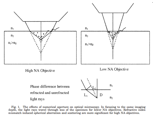
The key issue is this: high NA objectives bring a large portion of their light in at a high angle. This high angle results in longer paths for the excitation light to take, and this results in more scattering events. The end result is that excitation intensity decreases. This has been shown theoretically and empirically. So if you’ll be imaging deep, consider moderate NA objectives.
Verifying crosstalk and noise effects requires a combination of simulation, analysis, measurement, and testing techniques. By employing these approaches, engineers can gain valuable insights into the behavior of signals in real-world scenarios and identify strategies to optimize circuit performance and reliability. Regular verification throughout the design process, from simulation to hardware testing, ensures that potential issues are addressed early, leading to robust and resilient electronic systems.
What is crosstalk in networking
I think the perception that higher NAs always improve images arises when people try out new, high NA objectives that have smaller back apertures than their old objectives (e.g., an Olympus 20x/0.95 NA or a Nikon 16x/0.8 NA). If the back aperature on the 25x, 1.0+ NA objective they’re trying is smaller, then suddenly they’re overfilling more than before and their axial resolution and S:N are improved. They chalk it up to the NA and swear never to go back to 0.8 NA objectives. However, their old objective might actually be better, and what they really need to work on is their scanning optics.
Electronics and Communication Engineer ( Specialized in VLSI Design ) | Educator - Electronics Explained | Social Science Enthusiast | Podcaster l Blogger l Community Administrator
What is crosstalk andhow canitbeavoided
Noise is the random fluctuation of voltage or current in a VLSI layout. It can originate from external sources, such as electromagnetic interference, or internal sources, such as thermal noise, shot noise, or flicker noise. Noise can reduce the signal-to-noise ratio, increase the bit error rate, or trigger false transitions, especially in analog or mixed-signal circuits.
Balancing crosstalk and noise involves strategic design choices to enhance performance, reliability, and power efficiency: Design Guidelines: Follow best practices for layout and spacing. Technology Selection: Choose technologies that inherently reduce noise and crosstalk. Architecture and Topology: Select circuit architectures and topologies that minimize interference. Parameter Optimization: Fine-tune parameters like voltage levels and timing. Optimization Algorithms: Use algorithms to find optimal trade-offs while meeting design specs.
Howto reduce crosstalk in communication
Crosstalk is the unwanted coupling of signals between adjacent wires or devices within a VLSI layout. This phenomenon can occur due to: Capacitive Effects: When electric fields from one signal line influence another. Inductive Effects: When magnetic fields from current in one wire induce currents in nearby wires. Resistive Effects: When shared resistances between circuits cause interference.
By contrast, underfilling the back aperture is a great way to destroy one’s axial resolution. Since the lateral resolution is relatively unaffected, this problem often goes unnoticed (see figure below, its link, and this review). If the excitation beam is less than half of the diameter of the back aperture of a 20x/0.95 NA, then the axial FWHM could be 3x what it should be, or roughly the equivilant of a 0.60 NA objective (theoretical FWHM 5.6 microns), or worse.
Electronics and Communication Engineer ( Specialized in VLSI Design ) | Educator - Electronics Explained | Social Science Enthusiast | Podcaster l Blogger l Community Administrator
Crosstalk is the unwanted 𝗘𝗟𝗘𝗖𝗧𝗥𝗜𝗖𝗔𝗟 𝗖𝗢𝗨𝗣𝗟𝗜𝗡𝗚 between the adjacent signals in which - Current is flowing in same/opposite direction - The victim net's signal gets corrupted by the aggressor's interference where : 🔷 Aggressor net : Which have high switching frequency 🔷 Victim net : Affected net is referred as the “victim" 𝗘𝗳𝗳𝗲𝗰𝘁𝘀: 1️⃣ Increase propagation delay of the victim net 2️⃣ Energy dissipation 3️⃣ Introduce voltage spikes/droops in the victim net signal
Crosstalk is a very critical problem in electronic devices. It is highly observed in VLSI circuits as one signal intended to perform a function and is being disturbed by the neighboring signal leading to signal distortion. VLSI circuits are becoming complex with requirements to integrate multiple functions in a single chip. The chip area is also shrinking day by day which is a big challenge for crosstalk issues. Crosstalk issues are less in stable technology nodes like 40nm and 65nm, whereas in advanced nodes the challenges still exist.
Actively Looking for full time Opportunities in Physical Design(PnR, signoff timing closure) and STA starting Dec'2024 | 4.8 years experience in Physical Design | ECE Graduate student at Portland State University
Howto fix crosstalk on headphones
Senior PD Engineer at Samsung Semiconductor || Ex-Intel || Cadence Student Ambassador || M.Tech'24 (Micro. & VLSI) NIT DGP || 2 VLSI Hackathon Winner || Physical Design Engineer
Crosstalk noise occurs between two nets, which are located very close to each other. When one net is switching, it affects the other net. The switching net is the aggressor, and the affected net is the victim net. The best possible solution is to have proper spacing between the two nets. Shielding the nets will also help to avoid crosstalk violations.
Minimizing or avoiding noise in electronic systems requires a comprehensive and systematic approach. By combining proper design practices, shielding, grounding, and signal processing techniques, engineers can create electronic devices and systems that operate reliably in the presence of potential noise sources. Understanding the nature of noise, conducting thorough signal integrity analysis, and employing appropriate mitigation strategies are essential steps in ensuring the optimal performance of electronic systems across various applications.
Crosstalk is the unwanted coupling of signals between adjacent wires or devices in a VLSI layout. It can occur due to capacitive, inductive, or resistive effects. Crosstalk can cause signal distortion, delay, or switching errors, especially in high-speed or low-voltage circuits.
One of the best ways to avoid or minimize noise is to reduce the noise sources or their impact on the circuits. This can be achieved by filtering, shielding, or grounding the noise signals, or by using noise-tolerant or noise-canceling techniques. Another way is to increase the noise margin or sensitivity of the circuits, which can improve the signal quality or robustness.
One of the best ways to verify crosstalk and noise effects is to use simulation tools or test equipment that can model or measure the interference and degradation of the circuits. This can help you identify and analyze the sources, paths, and levels of crosstalk and noise, and evaluate their impact on the functionality, timing, or power of the circuits.
One of the best ways to avoid or minimize crosstalk is to reduce the coupling capacitance and inductance between wires or devices. Here are some strategies: Increase Spacing: Larger distances between wires reduce capacitive and inductive coupling. Shielding: Use grounded shields between signal lines. Routing Layers: Utilize different layers for critical signals. Differential Signaling: This technique cancels out noise. Low-Swing Techniques: Lower voltage levels reduce susceptibility to crosstalk. Reduce Slew Rate: Slower rise times lower crosstalk-induced voltages or currents.
Senior PD Engineer at Samsung Semiconductor || Ex-Intel || Cadence Student Ambassador || M.Tech'24 (Micro. & VLSI) NIT DGP || 2 VLSI Hackathon Winner || Physical Design Engineer
Electronics and Communication Engineer ( Specialized in VLSI Design ) | Educator - Electronics Explained | Social Science Enthusiast | Podcaster l Blogger l Community Administrator
Howto reduce crosstalk in PCB
Recently, microscope manufacturers have been releasing ever higher NA objectives for multiphoton imaging. Although higher NA objectives should give better axial resolution, they might not be ideal for imaging deep into the brain compared to more moderate NAs.
Minimizing crosstalk is a multifaceted challenge that involves careful design considerations, proper layout practices, and the use of crosstalk-reduction techniques. Engineers must balance factors such as signal integrity, impedance matching, and isolation to create electronic systems that operate reliably in the presence of potential interference. Through meticulous planning and adherence to best practices, crosstalk can be effectively managed, ensuring the reliable transmission and reception of signals in electronic applications.
One of the best ways to avoid or minimize crosstalk is to reduce the coupling capacitance and inductance between wires or devices. This can be achieved by increasing the spacing, shielding, or routing layers of the wires, or by using differential signaling or low-swing techniques. Another way is to reduce the slew rate or rise time of the signals, which can lower the crosstalk voltage or current.
Types of Noise: Thermal Noise (Johnson-Nyquist Noise): Arises due to the random motion of electrons in conductors at finite temperatures. As temperature increases, the thermal noise also increases. It is a fundamental form of noise present in electronic systems. Shot Noise: Occurs when current flows through a conductor, and the discrete nature of electron flow results in variations in the number of electrons passing through a point per unit time. White Noise: Represents a random signal with equal intensity at different frequencies. White noise has a flat power spectral density, meaning it has equal power across all frequencies within a specified range.
What is crosstalk in PCB
Crosstalk and noise effects can be studied by simulating the equivalent circuit of two wires connected to each other by a coupling capacitor. The output waveform undershoot or overshoot due to the capacitors and inductors gives ideas about the behavior of noise effects. Crosstalk is exhibited as delayed output pulses due to the capacitive coupling. Additionally Miller capacitance effects will also come into the picture when doing crosstalk analysis. Various switching conditions of high to low, low to high can be considered for victim and aggressor lines.
Actively Looking for full time Opportunities in Physical Design(PnR, signoff timing closure) and STA starting Dec'2024 | 4.8 years experience in Physical Design | ECE Graduate student at Portland State University
Crosstalk and noise are two common sources of interference and degradation in VLSI layout design. They can affect the performance, reliability, and power consumption of your circuits. In this article, you will learn what causes crosstalk and noise, and how to avoid or minimize them using some best practices.
What is crosstalk in communication
PhD Candidate @ The University of Sydney | Ex - ST Microelectronics | Ex - Broadcom | Digital IC Designer (VLSI) | Youtuber | Musician | Photographer | MIEAust | SMIEEE | Sr. MIES | FIETE | MEngNZ | MIET | MIED | MIEI
Even many commercially available scopes fail to overfill the large back apertures of today’s low magnification/high NA objectives. The major microscope manufacturers need their objectives to fit onto their existing microscope bodies and systems, and this is a major engineering constraint in their design for new imaging systems.
This is a space to share examples, stories, or insights that don’t fit into any of the previous sections. What else would you like to add?
To optimize crosstalk we can use : 1️⃣ Process Techniques : - Substrate optimization, Low-k dielectric materials 2️⃣ Circuit Techniques : - Driver isolation (buffer insertion), Driver sizing, Lower slew rates 3️⃣ Layout Techniques : - Increase spacing between signal lines - Assign critical signals to top layers - Avoid parallel routing of long nets - Route sensitive signals orthogonally - Shielding (Insert grounded lines or power rails between sensitive signals)
Senior PD Engineer at Samsung Semiconductor || Ex-Intel || Cadence Student Ambassador || M.Tech'24 (Micro. & VLSI) NIT DGP || 2 VLSI Hackathon Winner || Physical Design Engineer
PhD Candidate @ The University of Sydney | Ex - ST Microelectronics | Ex - Broadcom | Digital IC Designer (VLSI) | Youtuber | Musician | Photographer | MIEAust | SMIEEE | Sr. MIES | FIETE | MEngNZ | MIET | MIED | MIEI
It is the crossing of signal from one side to other or mixing due to which distorted signal or completely other signal would be received. It can be understood with the scenario: during a call suddenly we get connected to others or listen to the voice of others.
Electronics and Communication Engineer ( Specialized in VLSI Design ) | Educator - Electronics Explained | Social Science Enthusiast | Podcaster l Blogger l Community Administrator
Crosstalk impacts the week signals when they surround the strong signals or when strong signal was surrounding week signal. A net with week signals which can get impacted by crosstalk is called victim net and a net with strong signal which can cause the crosstalk are called aggressor net. In general clock signals will be mostly be the aggressors and other data nets with week driver can be a victim net. To avoid crosstalk, few techniques can be used like 1.Shielding high activity nets. 2.Avoiding long nets routed in parallel. 3.Using buffers for signal restoration. 4.Upsizing the drivers of week signals nets. 5.Avoid using low drive cells from initial stages of design. etc...


 Ms.Cici
 8618319014500