
All About Diffraction Gratings - diffraction film
Image lensiphone
These new application cases will have to balance the laser parameters we described early—tunability, purity, size, environmental resistance, power—depending on their material platforms, system architecture, and requirements. Some will need external lasers; some will want a fully-integrated laser. Some will need multi-laser arrays to increase capacity; others need more stringent temperature certifications.
Silicon is not a material that can naturally emit laser light from electrical signals. Decades of research have created silicon-based lasers with more unconventional nonlinear optical techniques. Still, they cannot match the power, efficiency, tunability, and cost-at-scale of lasers made from indium phosphide (InP) and III-V compound semiconductors.
GoogleLensonline
The tunable laser is a core component of all these tunable communication systems, both direct detection and coherent. The laser generates the optical signal modulated and sent over the optical fiber. Thus, the purity and strength of this signal will have a massive impact on the bandwidth and reach of the communication system. This article will clarify some critical aspects of laser design for communication systems.
Following these trends, at EFFECT Photonics, we are not only developing the capabilities to provide a complete, coherent transceiver solution but also the external nano-ITLA units needed by other vendors.
Googleimagesearch
The combination of tunable lasers and dense wavelength division multiplexing (DWDM) allows the datacom and telecom industries to expand their network capacity without increasing their existing fiber infrastructure. Thanks to the miniaturization of coherent technology and self-tuning algorithms, many application cases—metro transport, data center interconnects, and future access networks—will eventually move towards coherent tunable pluggables.
The world is moving towards tunability. The combination of tunable lasers and dense wavelength division multiplexing (DWDM) allows the datacom and telecom industries to expand their network capacity without increasing their existing fiber infrastructure. Furthermore, the miniaturization of coherent technology into pluggable transceiver modules has enabled the widespread implementation of IP over DWDM solutions. Self-tuning algorithms have also made DWDM solutions more widespread by simplifying installation and maintenance. Hence, many application cases—metro transport, data center interconnects, and —are moving towards tunable pluggables.
© 2024 EFFECT PHOTONICS All rights reserved. T&C of Website - T&C of Purchase - Privacy Policy - Cookie Policy - Supplier Code of Conduct
Therefore, making a suitable laser for silicon photonics does not mean making an on-chip laser from silicon but an external laser from III-V materials such as InP. This light source will be coupled via optical fiber to the silicon components on the chip while maintaining a low enough footprint and cost for high-volume integration. The external laser typically comes in the form of an integrable tunable laser assembly (ITLA).
Using an external or integrated laser depends on the transceiver developer’s device requirements, supply chain, and manufacturing facilities and processes. At EFFECT Photonics, we have the facilities and expertise to provide fully-integrated InP optical systems with an integrated laser and the external laser component that a silicon photonics developer might need for their optical system.
Imagesearch

The promise of silicon photonics (SiP) is compatibility with existing electronic manufacturing ecosystems and infrastructure. Integrating silicon components on a single chip with electronics manufacturing processes can dramatically reduce the footprint and the cost of optical systems and open avenues for closer integration with silicon electronics on the same chip. However, the one thing silicon photonics misses is the laser component.
GoogleLens

In contrast, the InP platform can naturally emit light and provide high-quality light sources and amplifiers. This allows for photonic system-on-chip designs that include an integrated laser on the chip. The integrated laser carries the advantage of reduced footprint and power consumption compared to an external laser. These advantages become even more helpful for PICs that need multiple laser channels.
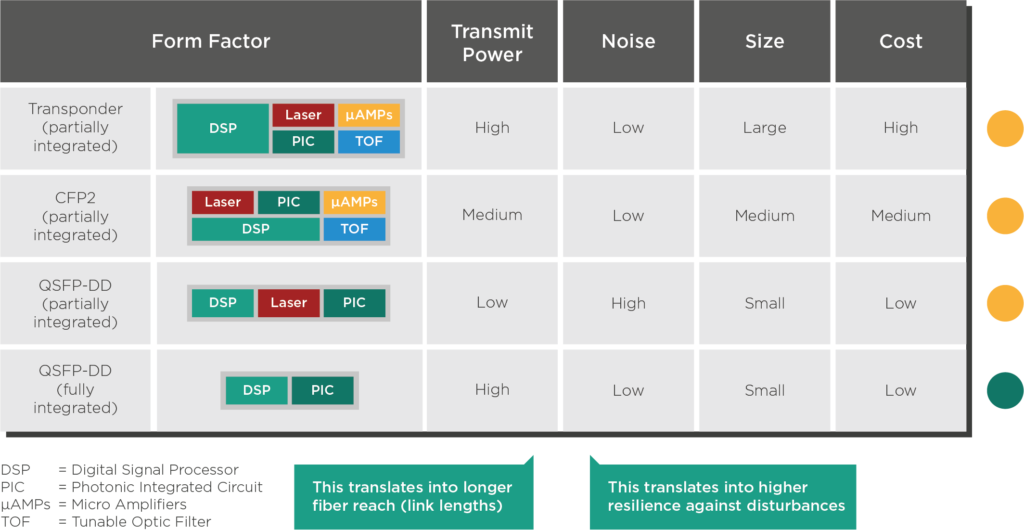
Image lensonline
Finally, integrated lasers enable earlier optical testing on the semiconductor wafer and die. By testing the dies and wafers directly before packaging them into a transceiver, manufacturers need only discard the bad dies rather than the whole package, which saves valuable energy, materials, and cost.
Earlier this year, Intel Labs demonstrated an eight-wavelength laser array fully integrated on a silicon wafer. These milestones are essential for tunable DWDM because the laser arrays can allow for multi-channel transceivers that are more cost-effective when scaling up to higher speeds.
In his recent talk at ECOC 2022, our Director of Product Management, Joost Verberk, outlined five critical parameters for laser performance.
Multi-laser array and multi-channel solutions will become increasingly necessary to increase link capacity in coherent systems. They will not need more slots in the router faceplate while simultaneously avoiding the higher cost and complexity of increasing the speed with just a single channel.


 Ms.Cici
 8618319014500