
690nm Red Collimated Laser System - collimated laser light
Cmos in cameraiphone
All returns must be authorized by Motic Instruments in order to insure proper credit and must be requested within 15 days of purchase. All returns may be subject to a 25% restocking charge and any cancellations may be subject to a cancellation fee. For returns not due to Motic error, the customer is responsible for all transportation fees related to the returned product. Should a return be granted, the purchase amount less shipping & handling fee and other applicable fees (restocking charge) will be deducted.
CMOSsensor
A figure of merit in CCD detectors known as "charge transfer efficiency" is how well the charge can be transferred to neighboring pixels without loss. In modern CCDs, the charge transfer efficiency is greater than 99.99%. In other words, the charge lost in the last pixel due to clocking is less than 0.01%. CCDs generally suffer from less fixed-pattern noise than CMOS detectors because unlike CMOS detectors, all the readout is performed by a single amplifier. Some CCDs use multiple amplifiers and divide the detector into regions read out by each amplifier with different possible architectures.
Yes it's all done in the sensor IC. CMOS and CCD detectors get their names specifically for how they do what you're asking. At their cores, they are both photovoltaic sensors and use the same physics to measure light and convert it to electricity.
CCDs work by building capacitance into each photodiode. The camera integrates (i.e. exposes) each pixel simultaneously for a fixed period. After the integration period, the charge on each pixel is shifted toward a readout amplifier using a process called "clocking." The first row of the CCD is read out by shifting each pixel down that row until the row is empty. Then each successive row is shifted up and the process is repeated. The clocking itself is performed by adding a bias voltage to an empty cell to attract the charge in a neighboring cell. One technique to select where the bias voltage is applied is to use an analog mux, but the mux is built into the die and optimized for the CCD readout architecture.
CMOSfull form
While SHUTTER is high, photodiode current is shunted into it (from any/all connected rows/columns, or in general as shown here), and when low, photocurrent charges the capacitors as usual. We can take an exposure by holding this high, reading out all the capacitors (resetting them), dropping it (letting charge accumulate for the desired time), then raising and reading out again. Since charge is stable (down to leakage / dark currents) with the "shutter" "closed", we eliminate the rolling-shutter effect, albeit at expense of reduced duty cycle and thus optical efficiency (we're not receiving signal during the readout phase), and continuity of observations (motion blur is now a discontinuous smear).
Overview. Zeiss Plan 40x/0.65 objective for 160mm tube length microscopes. Plan objectives are flatfield corrected and are the standard workhorse lenses for ...
This works well on a monolithic sensor, since although each capacitor and the charge it holds is tiny, the leakage paths are well-controlled. Trying to use these techniques with discrete parts on a PCB would be pretty much impossible.
A charge amplifier (i.e. op-amp integrator) would be effective here, with the ROWn edge falling rate controlled to avoid excess transient overshoot or peak currents in the amp. An integrator reset is also used to reset its value between pixels/rows.
In your design, you will want the per-pixel circuit to be as simple as possible, pushing as much of the complexity as possible to the edges (rows and columns) of the array. But if you really want simultaneous exposure for all pixels, there are limits to how simple the pixel circuit can be.
by M Mylonakis · 2018 · Cited by 19 — There are numerous methods to measure the diameter of a Gaussian laser beam, most of which are based on either direct imaging of the beam intensity profile or a ...
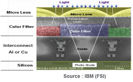
You are right that having readout circuitry for each pixel takes up area that could be used for detection. A figure of merit for CMOS detectors is the pixel "fill factor." A common fill factor for a modern CMOS detector would be about 30%. To account for this apparent loss in responsivity, CMOS detector manufacturers also put "microlenses" over each pixel to try to focus the light onto the light-sensitive part of the pixel.
Diodes are nice because they do a cromulent job of clamping/gating signals, and are available in dual pairs (e.g. BAV99DW, etc.). You also get one for free in the photodiode itself (give or take its capacitance, and whether photocurrent will be gated optically or electrically).
As background info, I'm an electrical engineer (power IC design) and photographer, and I'm designing my own camera (32x40 discrete pixels made of SMD photodiodes, will be about the size of a 4"x5" film holder). This is a personal project, and I consider the size, low resolution, and massive pain that will be involved in this as features. However, this is a challenging problem to solve for N=1280 pixels, and one that has been solved for N>1 billion by more clever engineers than me, so I thought I would try and learn from them. I do not want to dwell on the handling of color; I have my own solution for that (essentially a trichrome process that involves internally shifting a color filter between exposures).
Coherent is focused on delivering innovations that fuel market megatrends while pursuing our mission of enabling the world to be safer, healthier, closer, and ...
I understand conceptually how a pixel can work. A one-pixel camera is simple; you have a photodiode and measure its current, either through a TIA or an integrator, then convert that through an ADC to a signal. The trick is having multiple pixels and sensing them.
We could also think about displays, in which case a very similar scheme might be used to set the gate voltage on an array of transistors driving LEDs. The gates of course have capacitance, so we don't need a sample capacitor, and some diode arrays and row/col drivers can be used to set things up. ID vs. VGS is rather notoriously unreliable (typically varying by a volt or so, but a volt also varies ID by a decade or two at the sharpest point of the curve!), but this could be measured by setting each pixel hot in turn and reading supply current, or even intensity with a photodiode at a distance. It should be compensated for temperature, and maybe periodically for drift too, but may be stable enough to work practically (well, "practical" given these are impractical neat-o project ideas to begin with, that is ;) ).
All returns must be authorized by Motic Instruments in order to insure proper credit and must be requested within 15 days of purchase. All returns may be subject to a 25% restocking charge and any cancellations may be subject to a cancellation fee. For returns not due to Motic error, the customer is responsible for all transportation fees related to the returned product. Should a return be granted, the purchase amount less shipping & handling fee and other applicable fees (restocking charge) will be deducted.
The simplest way I can think of, is to use diode gates to steer charge around. A capacitor per pixel may be needed, but potentially the photodiode's own capacitance could be used (depending on how exposure is done, how fast/often readout can be performed, and desired sensitivity/dynamic range). That would probably be something like a mechanical or LCD shutter, versus electronically gating it.
Aspheric lens has a non-spherical lens surface. The main advantage of aspheric lenses is its ability to correct for spherical aberration. Aspheric lenses allow ...
I have some experience designing cameras with monolithic image sensors, so I can provide some insight. I think the question really boils down to this:
CMOSimage sensor working principle
Types ofcmos in camera
Lens Arrays are commonly used to spatially control the phase of a beam. Find and compare Lens Arrays, including Microlens Array and ...
At Motic Instruments, we take pride in the quality of our products and our user experience. That's why we offer technical advice and full post-sale support to keep your Motic products in optimal condition and ensure your microscopy results are of the highest quality. All of our microscopes are covered by a 5 year warranty on mechanical components and 1 year warranty on electrical components.
At Motic Instruments, we take pride in the quality of our products and our user experience. That's why we offer technical advice and full post-sale support to keep your Motic products in optimal condition and ensure your microscopy results are of the highest quality. All of our microscopes are covered by a 5 year warranty on mechanical components and 1 year warranty on electrical components.
CMOS Cameraprice
Since readout is destructive (capacitor voltage is reset to a diode Vf, give or take), we don't need a separate reset circuit. This will give a rolling-shutter effect, where the frame is scanned in a raster, rather than a synchronous snapshot. (Also a commercially-justifiable compromise.)
Assuming this would be supported by an MCU, or PC or FPGA for that matter, we can potentially tolerate quite gross behavior, as long as we still have adequate dynamic range for the signal in general. For example, we can calibrate out dark current and diode leakage by simply photographing a dark scene and subtracting those values from the readings; this also accounts for charge injection by the various diode junctions (or transistors, if we wish to use them for charge gating instead), which look like constant adders to the signal. Diode leakage currents will be proportional to exposure time, so a series of dark exposures could be taken, and used to calibrate with respect to that. If self-gating through the photodiodes themselves, photocurrent will be an error term in the charge measurement (i.e. since the measurement takes finite time, some current will be superimposed on the desired charge), but we can account for that as an error factor per pixel after calibrating the other effects out. And so on and so forth; if we have imperfect resetting between frames, we can subtract a (potentially nonlinear) fraction of the previous frame, and thus eliminate (or at least greatly reduce) tracking or motion blur. Other nonlinear functions can be employed as well, like gamma or log correction; a logarithmic amp could be used in the first place to maximize dynamic range at the array; or it could be variable-gain to act as electronic f-stop. Lots of possibilities.
by R Paschotta · Cited by 2 — Figure 1: Setup of a regenerative amplifier for picosecond pulses. A Pockels cell, combined with a quarter-wave plate and a thin-film polarizer (TFP), acts as ...
Note that the array can be folded into strips, so that for example if we only want to use two quad op-amps' worth of columns, we can introduce more rows, and weave the columns back and forth a few extra times. (Assuming we have enough layout area to do the layer changes and turn around the bus.) For example, a 32x40 array might use 8 x quad op-amps and 5 x octal decoders, but maybe we want to use 4 quad amps and 10 decoders -- because the decoders won't require resistors, capacitors, analog switches, etc. to support them. In this way, we can optimize the M+N as well as M*N component counts.
And, two or three components per pixel, is not too bad. And many of them can be arrays; quad capacitors, and dual or triple diodes (or dual pairs like the BAV99DW mentioned earlier) are common enough, and, photodiode arrays probably aren't suitable for obvious (mechanical) reasons, but if you can find some that are cheap and easily arranged in grids, that would be excellent.
As you can start to tell, trying to design either of these circuits with discrete components is impractical commercially, but could still be a good educational exercise using a method like the one proposed by Tim Williams. Modern CMOS detectors have pixel pitches less than 3 microns, meaning the detector and amplifier for each pixel all fit within a 3x3 micron area.
Bi-Concave Lens (BCC) ... Bi-concave lenses are useful for a wide range of beam expansion or negative imaging applications. These lenses are manufactured from ...
cmossensor vs full-frame
In very general terms, each pixel of a solid-state image sensor (CMOS or CCD) contains a moderately complex circuit involving several transistors. They control the integration of the photocurrent into a capacitor, the transfer of that charge onto a bus or analog shift register and the resetting of the integration capacitor.
HeyOptics USB 3.0 Fiber Optic Extender adopts detachable MPO fiber connector to reach up 1000ft (303 meters) transmission and features a small size ...
Conversely, CMOS detectors have a CMOS amplifier circuit built into each pixel. After integration, an external (still internal to the IC but external to the pixels) circuit addresses the pixels onto an analog mux to an ADC or in some cases additional amplifiers before going to an ADC. This is often done on several channels to multiple ADCs after which the pixels are interleaved together to reform the image.
We could even put the photodiode anodes on the columns directly, since they are diodes themselves; this introduces more error from photocurrent during the readout plus charge injection due to their relatively large junction capacitance (particularly at low bias voltage; notice they're kept at 5-10V reverse bias in the above description, which helps optimize photocurrent and capacitance).
Stack Exchange network consists of 183 Q&A communities including Stack Overflow, the largest, most trusted online community for developers to learn, share their knowledge, and build their careers.
Normally, ROWn are held high (+10V say), and COLn are held halfway (+5V say). In this condition, photocurrents charge the capacitors (example values shown), at least until they reach 5V (at which point the COLn diodes begin to turn on, and you get a visual blowout effect where a bright spot seems to smear across all rows; many real cameras have this effect, so this seems an acceptable compromise). To read out a row of pixels, drop the respective row to +5V, and read current on the COLns. We read columns in parallel to keep bandwidth high, or use an analog switch/mux to select one at a time (their charges should be reasonably stable while we scan a given row; of course if not, that's another source of error).
Or we could put the photodiodes on the columns, ignoring the total photocurrent (or on the assumption that it's very small on average, compared to the pulsed signal current/charge), and using them as the column readout diode.
CMOSvs CCD
Position the nosepiece so that the lowest scanning (4X) objective is in place. ... OCULAR LENS or EYEPIECE — On a binocular scope there are two ocular lenses,.
As for optical efficiency, if very wide-area photodiodes are used, much of the space between pixels could potentially be covered, and a both-sided PCB assembly could be used to carry all the components. Alternately, THT photodiodes could be used, to stand up above the SMT components (though I suspect wide-area parts aren't so well available in such format?). Still other, an, I suppose planar variant of a bug eye could be made: a lens array could focus incident light onto a fairly small photodiode, leaving ample room for components around them. This greatly restricts how an image can be formed on the array, of course; but perhaps we treat this as a feature rather than a (ha!) bug, and angle the lenses to target a particular wavefront/direction, or adjust alignment between board and lens array to play with adjustable angle and focus, etc.
Do CMOS/CCD sensors just get away with doing this in the sensor IC, or is there an approach I'm missing here? Suggestions and insights welcome, as well as recs for future reading.
Beam Splitting and preparation for welding ... Beam Splitting. Sureway Metal Systems. 285120 Duff Drive SE Calgary AB, T1X 0K1 Phone: 403.287.2742. Fax ...
Obviously, these corrections become more and more onerous as you go up in resolution and frame rate, but an FPGA, or application CPU probably for that matter, can handle pretty much as big an array as you might care to construct out of discrete components, while costing a tiny fraction of the overall assembly.
My understanding is that CMOS sensors have photosites for each of their pixels, which are essentially photocapacitors that accumulate an amount of charge proportional to light that hits them during an exposure. How does a digital camera sense and measure these without most of the die area being mostly analog muxes? How do they isolate the sites from each other so there's no crosstalk/pixels corrupting each other and adding parasitic capacitance/creating stray voltages in floating nodes when off? Is there one central gain circuit and TIA, or is it distributed?
Currently, the most sensible approach I can think of is to analog mux the anodes and cathodes of my photodiodes (so an MxN array of diodes requires an M-channel mux for the cathodes and an N-channel mux for the anodes), but this would mean I could only measure one site at a time. Another approach would be to use a photosite approach where each diode gets a capacitor and each cap is measured and reset at the end of an exposure, but this requires figuring out how to turn off all the sites at the end of image capture so they can preserve their voltages while the rest are scanned through, as well as figuring out how to analog mux 1280 separate nodes to one ADC (or multiple ADCs, but it wouldn't lower the mux count much). The advantage is that your image sensor now has the whole exposure time to store photons, effectively raising your ISO by a factor of 1280 in this case and eliminating the rolling shutter effect.


 Ms.Cici
 8618319014500