
200+ Best Gym Quotes (Motivational & Funny) - exercise quotation
A fully equipped measurement laboratory is available to ensure that the end product will meet the initial specifications of your project.
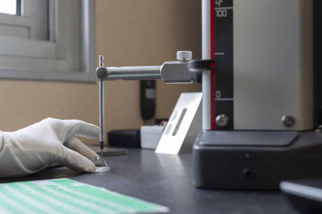
Using several tools ranging from mechanical sensors to 3D camera vision systems, the metrology laboratory performs the complex task of measuring and qualifying high-precision transparent parts.
The new WILDSUN-K25 TC is particularly suitable for meeting the stringent lighting demands of sporting events, shows or any prestigious events requiring high-quality light and perfectly rendered color.
Achieving nanometers in machining requires metrology equipment to achieve the same level of accuracy. This dedicated laboratory assesses the parts during the first stages of the prototyping of the injection process but also serves as a quality management tool for the control of production batches and the analysis of the root causes of possible injection drifts.
ExtremeUV wavelength
The breakthrough will have implications for attosecond physics, as the metalens can be used to better understand light and matter interactions on the nanoparticle scale. Capasso says the semiconducting industry will also benefit from EUV metalens technology because it will enable the fabrication of smaller and smaller transistors and processors. But, perhaps most exciting, Capasso says there are likely many future applications that haven’t yet been thought of.
Academics, Applied Physics, Alumni, Bioengineering, Diversity / Inclusion
Extreme ultravioletlithography machine
The idea was originally conceived by Marcus Ossiander, a postdoctoral fellow in Capasso’s group, whose background is in attosecond physics, or the study of how light and matter interact on the inconceivably-small timescale of quintillionths of a second. “The only way you can create laser pulses on the attosecond scale is using these very short wavelengths of ultraviolet light,” Ossiander says. “I had this big dream, a bit of a moonshot, really, to create a metalens that could control EUV. And Federico will never stop you from pursuing a dream.”
A new perforated metalens proves it is possible to use nano-optics to focus beams of extreme ultraviolet light (EUV) and could open new doors in microscopy, sensing, holography, and fundamental physics research. The advance is reported in Science.
“This work really pushed the limits of what’s possible in nanotechnology today,” Capasso says. “We needed impeccable fabrication methods to make this metalens with features small enough to interact with EUV wavelengths, which means the features must be smaller than those wavelengths. It pushed us to shrink the metalens features by a factor of 10 compared to what’s been done before – it was really a very large leap.”
“Every element [of this project] worked like in an orchestra,” Meretska says. “Both sample fabrication and measurement processes are incredibly challenging and knowing everything worked as designed was very satisfying.”
Our modern and spacious warehouse allows a security stock for all standard products, as well as the parts from your custom project according to our logistics agreement.
“Why not flip the design… to make transmissive pillars… out of air?” he says. By making holes in the surface of a material with a lower refractive index than air itself, he hypothesized that EUV could be guided and focused using the vacuum inside the holes. When computer simulations suggested it might actually work, he teamed up with nanofabrication expert Maryna Leonidivna Meretska, a postdoctoral researcher in Capasso’s lab, to develop a prototype.
Extreme ultravioletlithography
ASTERA AX5 45W RGBW (3x15W) with an angle of 13°. Optimized for a quick return on investment, this stage light now replaces all wireless and wired PARs and batteries. It is the ultimate tool for entertainment professionals.
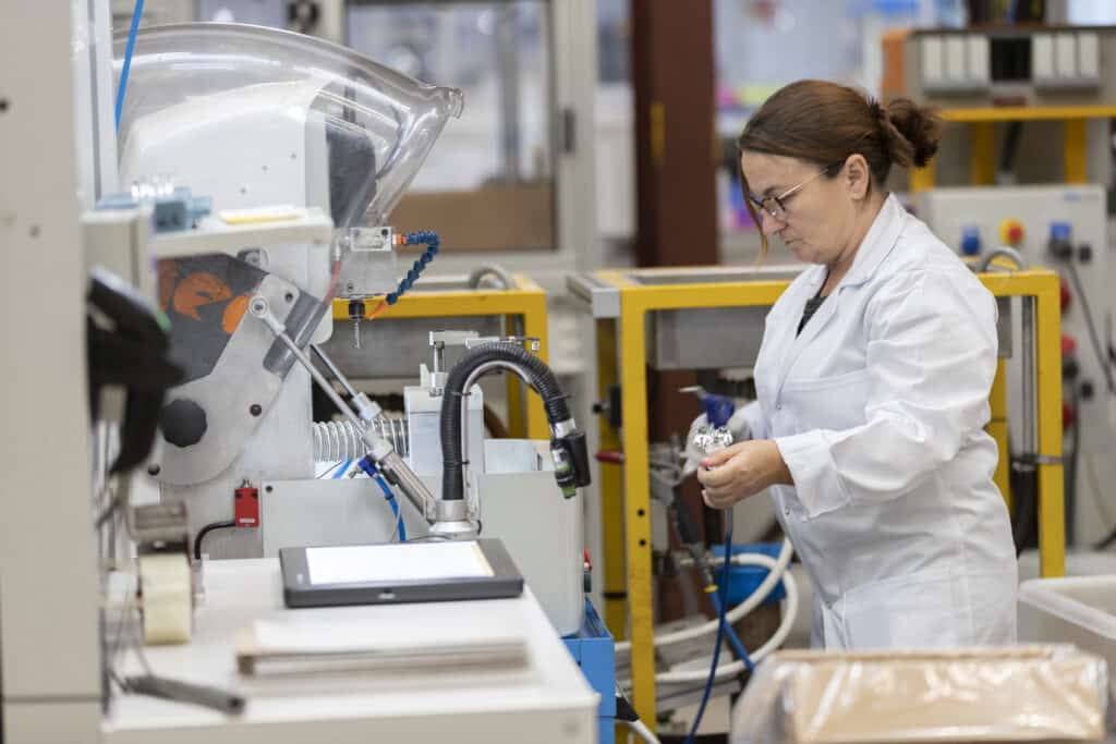
Our high-precision machines driven by qualified engineers provide the optical quality required for the perfect duplication of the optical pattern on plastic parts.
MAGICPANEL-FX is the exciting new multi-function, multi-use luminaire descended from the renowned MAGICPANEL-R. With a revolutionary new optical zoom system that has no visible moving parts and a stationary transmitting lens, this proprietary system has a 15:1 zoom ratio with a range of 3.6° to 53°.
We can adapt the automation level according to the characteristics of the project, price, and quality requirements. For example, an automatic pre-packaging process using collaborative robots is available if the parts are to be kept away from human contact or interaction.
Extreme ultravioletlithography companies
Typical metalenses rely on the fabrication of nanopillars that – sticking up like the skyscrapers of the Manhattan skyline – refract visible light and focus it in desired ways. But with EUV light being absorbed by all materials it reaches, Ossiander knew that strategy would not work. As he contemplated the way materials interact with light that oscillates incredibly fast, a creative new idea struck him.
Follow our product launches at the rate of maximum one email per month. We will not share your information with any third party, and you can unsubscribe at any time. Access our past newsletters.
Our injection workshop is equipped with presses from 35 to 500 tons. We provide state-of-the-art injection capacity, based on our extensive experience in transparent plastic and silicone injection, whatever the injected material and the project.
Ultraviolet lightfrequency
Depending on the goals and specifications of your project, our team of optical engineers will work with you to obtain the best possible performance, taking into account the constraints of the injection process that must be integrated into the first stages of development.
Deepultravioletlithography
The roughness of the finishing surface is achieved thanks to the golden hands of our polishers. All these capabilities and equipment combined with our expertise in tool design offer the best guarantee of robust and accurate tooling.
“We don’t currently know all the fields that might benefit from EUV metalenses, because no one expected that this type of technology would be possible anytime soon,” Ossiander says.
Harvard’s Office of Technology Development has protected the intellectual property arising from this study and is exploring commercialization opportunities.
It takes a lot of different know-how to move from an idea to a practical industrial solution. With more than 40 years of experience in optical solutions design and parts injection, we provide the best possible service at all stages of the project. From the early stages of optical design to parts shipping and logistics, we do our best to provide the best customer experience in its class.
We accompany you from the initial phase of your project thanks to an integrated optical research and development department.
Since that initial metalens demonstration, researchers far and wide have been adopting the technique to create metalens designs that exert increasingly complex control over visible and infrared light – but harnessing such metasurfaces to control light in the EUV range has remained out of reach. EUV wavelengths are extremely small, around the 50-nanometer range, which is much smaller than visible wavelengths of light, which are 400 to 700 nanometers in size. At such a small wavelength, EUV is absorbed by all materials, preventing that light from being refracted and controlled by transmissive optics.
Ultraviolet lightexamples
At the Harvard John A. Paulson School of Engineering and Applied Sciences (SEAS), Federico Capasso’s lab unveiled in 2011 the groundbreaking concept of refracting metasurfaces, or sub-wavelength-spaced arrays of nanostructures, with a Science paper that has since been cited 7,000 times. In 2016, another Science paper reported the use of high-performance flat lenses made up of nanopillars and fabricated using lithography techniques, which unlocked a new strategy to focus light. That work was a major leap forward for conventional optical devices that had historically been fabricated by molding, making them thick and bulky.
Delivering parts on time and ensuring good transport and protection conditions is the final step in our daily quality commitment.
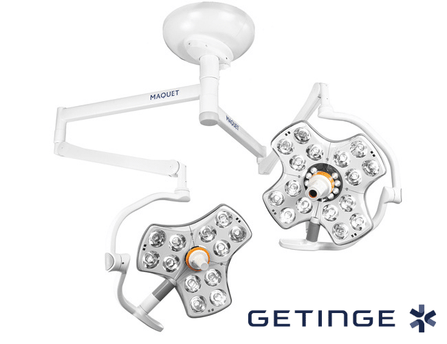
MAQUET / GETINGE is a leading global provider of products and systems that contribute to quality enhancement and cost efficiency within healthcare and life sciences. They employ more than 15,500 people and have operations in 41 countries.
Ultraviolet lightwavelength
We are immensely proud that so many companies trust us with their optical parts needs. From street lighting to architecture, medical and entertainment, The Gaggione team has worked with the most important players in each field. Whatever the application, we are fully committed to giving the entire project the attention and professionalism it deserves. Here are some examples of partnerships and specific products we have worked on:
Once the prototype was complete, Ossiander flew to the Institute of Experimental Physics at Graz University of Technology in Austria, one of few labs in the world that can create EUV. There, researchers led by attosecond physicist Martin Schultze (a co-corresponding author on the study) sent EUV radiation through the metalens prototype. After many experiments, the team saw what they had long dreamed of: a small spot, indicating the concentration of light, detected by a special camera.
On our optical components, roughness can be reduced to 5 nm while surface accuracy can reach λ/4 on a 150 mm diameter thanks to the ultra-precision lathe. If a free-form geometry is required, our machines allow us to perform high-speed milling that can achieve a surface accuracy of 1µm on components with a roughness of a few tenths of a nanometer.
The Capasso group’s latest breakthrough – fabricating a metalens that uses nano-sized holes to vacuum-guide EUV -- introduces a game-changing workaround. “This work will revolutionize optics in a spectral region (extreme UV) where, until now, there were no lenses or viable optics for high-performance or high-volume applications,” says Capasso, co-corresponding author, who is the Robert L. Wallace Professor of Applied Physics and Vinton Hayes Senior Research Fellow in Electrical Engineering at SEAS. The new work was in collaboration with Martin Schultze’s lab at Graz University of Technology.
“Fabrication, in general, requires a lot of perseverance,” Meretska says. “It took many attempts to realize the working sample. We learned something new about the process with every attempt, and that kept me going.”
Part of this work was performed at Harvard’s Center for Nanoscale Systems (CNS), a member of the National Nanotechnology Coordinated Infrastructure (NNCI), which is supported by the NSF under award no. ECCS-2025158. Computations were run on the FASRC Cannon cluster supported by the FAS Division of Science Research Computing Group at Harvard University. This research was supported by the Alexander von Humboldt Foundation (Feodor-Lynen Fellowship), the Austrian Science Fund (FWF, Start Grant Y1525), the European Union (grant agreement 01076933 EUVORAM), A*STAR Singapore through the National Science Scholarship Scheme, and the Air Force Office of Scientific Research (AFOSR) under award Number FA9550-21-1- 0312.
With our extensive experience and resources, we offer a complete design, development and manufacturing service to produce custom optical parts and systems. We also carry a constantly evolving standard range suitable for numerous applications. Our constant quest for innovation has resulted in the patenting of several technologies.


 Ms.Cici
 8618319014500