
Mechanical Engeniring - Academia.edu - engeniring
Darkfield vs brightfieldreddit
The dynamic range of a CMOS image sensor is determined by the maximum number of signal electrons accumulated by the photodiodes (charge capacity) divided by the sum of all components of sensor read noise (noise floor), including temporal noise sources arising over a specific integration time. The contribution from all dark noise sources, such as dark current noise, as well as pixel read noise, and temporal noise arising from the signal path (but not photon shot noise), is included in this calculation. The noise floor limits image quality in dark regions of the image, and increases with exposure time due to dark current shot noise. In effect, therefore, the dynamic range is the ratio of the largest detectable signal to the smallest simultaneously detectable signal (the noise floor). Dynamic range is often reported in gray levels, decibels or bits, with higher ratios of signal electrons to noise producing greater dynamic range values (more decibels or bits). Note that dynamic range is governed by sensor signal-to-noise characteristics, while bit depth is a function of the analog-to-digital converter(s) employed in the sensor. Thus, a 12-bit digital conversion corresponds to slightly over 4,000 gray levels or 72 decibels, while 10-bit digitization can resolve 1,000 gray levels, an appropriate bit depth for a 60-decibel dynamic range. As the dynamic range of a sensor is increased, the ability to simultaneously record the dimmest and brightest intensities in an image (intrascene dynamic range) is improved, as are the quantitative measurement capabilities of the detector. The interscene dynamic range represents the spectrum of intensities that can be accommodated when detector gain, integration time, lens aperture, and other variables are adjusted for differing fields of view.
Brightfieldmicroscope
Electronic shuttering in CMOS image sensors requires the addition of one or more transistors to each pixel, a somewhat unpractical approach considering the already compromised fill factor in most devices. This is the case for most area-scan image sensors. However, line-scan sensors have been developed that have shutter transistors placed adjacent to the pixel active area in order to reduce the fill factor load. Many designers have implemented a nonuniform rolling shutter solution that exposes sequential rows in the array at different time intervals utilizing a minimum of in-pixel transistors. Although rolling shutter mechanisms operate well for still images, they can produce motion blurs leading to distorted images at high frame rates. To solve this problem, engineers have crafted uniform synchronous shutter designs that expose the entire array at one time. Because this technique requires extra transistors at each pixel, there is some compromise of fill factor ratios unless larger pixels are simultaneously implemented.
Much of the latest news surrounding machine vision is about machine learning and the innovations regarding algorithms. But those algorithms need data to perform correctly. The data in this case is the images. It is imperative to capture the best image possible so that the algorithms can perform at their highest level.
Because CMOS image sensors are capable of accessing individual pixel data throughout the entire photodiode array, they can be utilized to selectively read and process only a selected portion of the pixels captured for a specific image. This technique is known as windowing (or window-of-interest readout), and dramatically expands the image-processing possibilities with these sensors. Windowing is controlled directly on the chip through the timing and control circuit, which enables any size window in any position within the active region of the array to be accessed and displayed with one-to-one pixel resolution. This feature can be extremely useful when temporal motion tracking of an object in one subregion of the image is necessary. It can also be employed for on-chip control of electronic pan, zoom, accelerated readout, and tilt operations on a selected portion or the entire image.
The unbalanced nature of Bayer filter mosaic arrays, having twice as many green filters as blue or red, would also appear to present a problem with regards to accurate color reproduction for individual pixels. Typical transmission spectral profiles of the common dyes utilized in the construction of Bayer filters are presented in Figure 4. The quantum efficiency of the red filters is significantly greater than that of the green and blue filters, which are close to each other in overall efficiency. Note the relatively large degree of spectral overlap between the filters, especially in the 520 to 620 nanometer (green, yellow, and orange) region.
Dark field lighting photography
These four short wave infrared (SWIR) pictures show how machine vision designers can use this spectral band to see through paint and differentiate between materials. The two bottles show in images 1 and 2 show alcohol and water, with clear alcohol clearly differentiated in the second image. In the second pair of images, SWIR radiation is able to penetrate the paint on the plastic card, revealing the patterns underneath. This technique is widely used in ports for detecting altered storage containers.
Although many CMOS fabrication plants lack the process steps for adding color filters and microlens arrays, these steps are being increasingly implemented for image sensor production as market demands grow. In addition, optical packaging techniques, which are critical to imaging devices, require clean rooms and flat-glass handling equipment not usually found in plants manufacturing standard logic and processor integrated circuits. Thus, ramp-up costs for image sensor fabrication can be significant.
Dome, or diffuse, illumination (also called cloudy-day illuminator). Think of dome lighting as a big bowl with a hole in the middle. The bowl sits upside down, so the camera is looking through the hole, and the light shines up into the bowl and scatters in every direction. Dome lighting is also called “cloudy-day illuminator.” Imagine being outside on a very cloudy but sunny day. Everything is bright and lit up, but there are no shadows because the clouds diffuse and disperse the light all over the place. This method works great for objects that have a lot of different angles, such as packaging (blister packs and poly bags).
General dark field illumination. The camera looks straight at the object, but the lighting comes in from the very lowest angles. Think of the part as the horizon and the lights as coming in right above the horizon. The light skims across the object and away from the camera. Any bump or dent is highlighted because the light hits it and bounces toward the camera. This method is very effective for highlighting objects with direct part markings.
CMOS image sensors are fabricated on well-established standard silicon processes in high-volume wafer plants that also produce related chips such as microprocessors, memory circuits, microcontrollers, and digital signal processors. The tremendous advantage is that digital logic circuits, clock drivers, counters, and analog-to-digital converters can be placed on the same silicon foundation and at the same time as the photodiode array. This enables CMOS sensors to participate in process shrinks that move to smaller linewidths with a minimum of redesign, in a manner similar to other integrated circuits. Even so, in order to guarantee low-noise devices with high performance, the standard CMOS fabrication process must often be modified to specifically accommodate image sensors. For example, standard CMOS techniques for creating transistor junctions in logic chips might produce high dark currents and low blue response when applied to an imaging device. Optimizing the process for image sensors often involves tradeoffs that render the fabrication scenario unreliable for common CMOS devices.
A closer look at the photodiode array reveals a sequential pattern of red, green, and blue filters that are arranged in a mosaic pattern named after Kodak engineer Bryce E. Bayer. This color filter array (a Bayer filter pattern) is designed to capture color information from broad bandwidth incident illumination arriving from an optical lens system. The filters are arranged in a quartet (Figure 2(a) and Figure 2(b)) ordered in successive rows that alternate either red and green or blue and green filters (Figure 2(a)). Presented in Figure 2 are digital images captured by a high-resolution optical microscope of a typical Bayer filter array and the underlying photodiodes. Figure 2(a) illustrates a view of alternating filter rows. Each red filter is surrounded by four green and four blue filters, while each blue filter is surrounded by four red and four green filters. In contrast, each green filter is surrounded by two red, four green, and two blue filters. A high magnification image of the basic repeating unit is presented in Figure 2(b), and contains one red, one blue, and two green filters, making the total number of green filters in the array equal to the number of red and blue filters combined. The heavy emphasis placed upon green filters is due to human visual response, which reaches a maximum sensitivity in the 550-nanometer (green) wavelength region of the visible spectrum.
General bright field illumination. Imagine a ring of light surrounding the camera, looking straight onto the object. Features that are flat and reflective will appear brighter than those that are curved or absorptive. This is great for looking at print on objects.
Backlight illumination. This method uses a flat diffuse light that comes from behind the part and is aimed directly at the camera. The object will block the light so it will appear dark and the background white. This allows the image to have very clear edges. This method is great for measurements and checking the fill level of liquids.
Pixel size has continued to shrink during the past few years, from the 10-20 micron giant pixels that ruled the mid-1990s devices, to the 6-8 micron sensors currently swamping the market. A greater demand for miniature electronic imaging devices, such as surveillance and telephone cameras, has prompted designers to drop pixel sizes even further. Image sensors featuring 4-5 micron pixels are being utilized in devices with smaller arrays, but multi-megapixel chips will require pixel sizes in the 3 to 4 micron range. In order to achieve these dimensions, CMOS image sensors must be produced on 0.25-micron or narrower fabrication lines. By employing narrower line widths, more transistors can be packed into each pixel element while maintaining acceptable fill factors, provided that scaling ratio factors approach unity. With 0.13 to 0.25-micron fabrication lines, advanced technology, such as in-pixel analog-to-digital converters, full-color processing, interface logic, and other associated complex circuitry tuned to increase the flexibility and dynamic range of CMOS sensors should become possible.
Reflection and transmission of incident photons occurs as a function of wavelength, with a high percentage of shorter wavelengths (less than 400 nanometers) being reflected, although these losses can (in some cases) extend well into the visible spectral region. Many CMOS sensors have a yellow polyimide coating applied during fabrication that absorbs a significant portion of the blue spectrum before these photons can reach the photodiode region. Reducing or minimizing the use of polysilicon and polyimide (or polyamide) layers is a primary concern in optimizing quantum efficiency in these image sensors.
Thus, each pixel (or imaging element) contains, in addition to a photodiode, a triad of transistors that converts accumulated electron charge to a measurable voltage, resets the photodiode, and transfers the voltage to a vertical column bus. The resulting array is an organized checkerboard of metallic readout busses that contain a photodiode and associated signal preparation circuitry at each intersection. The busses apply timing signals to the photodiodes and return readout information back to the analog decoding and processing circuitry housed away from the photodiode array. This design enables signals from each pixel in the array to be read with simple x,y addressing techniques, which is not possible with current CCD technology.
Difference between dark field and phase contrast microscopy
Photon shot noise is readily apparent in captured images as a random pattern that occurs because of temporal variation in the output signal due to statistical fluctuations in the amount of illumination. Each photodiode in the array produces a slightly different level of photon shot noise, which in the extreme can seriously affect CMOS image sensor performance. This type of noise is the dominant source of noise for signals much larger than the intrinsic noise floor of the sensor, and is present in every image sensor, including CCDs. Dark current is generated by artifacts that produce signal charge (electrons) in the absence of illumination, and can exhibit a significant degree of fluctuation from pixel to pixel, which is heavily dependent upon operating conditions. This type of noise is temperature-sensitive, and can be removed by cooling the image sensor or through an additional frame store, which is placed in random access memory and subtracted from the captured image.
Even though there are infinite possibilities of objects to inspect, with these steps you are well on your way to finding the right light to highlight the features needed for a great image. V&S
One of the major drawbacks of the three-pixel APS design is the relatively high level of an artifact known as fixed pattern noise (FPN). Variations in amplifier transistor gain and offset, which are a fundamental problem with CMOS technology process fluctuations during manufacture, produce a mismatch in transistor output performance across the entire array. The result is a noise pattern evident in captured images that is constant and reproducible from one image to another. In most cases, fixed pattern noise can be significantly reduced or eliminated by design tuning of analog signal processing circuitry located at the periphery of the array or by electronic subtraction of a dark image (flat-field correction).
Coaxial illumination. The camera looks straight at the object, and light comes in straight in-line with the camera. All the light that is in-line and hitting a flat surface will shine directly back up at the camera. Anything flat will be bright. Anything not flat will be dark because if the light hits an angled surface it reflects away from the camera. This method works really well for highlighting scratches or other surface defects.
In most CMOS photodiode array designs, the active pixel area is surrounded by a region of optically shielded pixels, arranged in 8 to 12 rows and columns, which are utilized in black level compensation. The Bayer (or CMY) filter array starts with the upper left-hand pixel in the first unshielded row and column. When each integration period begins, all of the pixels in the same row will be reset by the on-board timing and control circuit, one row at a time, traversing from the first to the last row catalogued by the line address register (see Figure 7). For a sensor device with analog output, when integration has been completed, the same control circuitry will transfer the integrated value of each pixel to a correlated double sampling circuit (CDS block in Figure 7) and then to the horizontal shift register. After the shift register has been loaded, the pixel information will be serially shifted (one pixel at a time) to the analog video amplifier. The gain of this amplifier is controlled either by hardware or software (and in some cases, a combination of both). In contrast, CMOS image sensors with digital readout utilize an analog-to-digital converter for every column, and conversion is conducted in parallel for each pixel in a row. A digital bus having a width equal to the number of bits over which the conversion is accomplished is then employed to output the data. In this case, only the digital values are "serially" shifted. White balance algorithms are often applied to the pixels at this stage.
Dark current is virtually impossible to eliminate, but can be reduced through the utilization of pinned photodiode technology during CMOS sensor fabrication. To create a pinned photodiode pixel, a shallow layer of P-type silicon is applied to the surface of a typical N-well photosensitive region to produce a dual-junction sandwich that alters the visible light spectral response of the pixel. The surface junction is optimized for responding to lower wavelengths (blue), while the deeper junction is more sensitive to the longer wavelengths (red and infrared). As a result, electrons collected in the potential well are confined near the N region, away from the surface, which leads to a reduction of dark current and its associated noise elements. In practice, it can be difficult to construct a pinned photodiode pixel that produces a complete reset in the low-voltage environment under which CMOS sensors operate. If a complete reset condition is not achieved, lag can be introduced into the array with a corresponding increase in reset transistor noise. Other benefits of pinned photodiode technology are improved blue response due to enhanced capture of short-wavelength visible light radiation in the vicinity of the P-silicon layer interface.
As an example of how color interpolation functions, consider one of the green pixels nested in the central region of a Bayer filter array. The pixel is surrounded by two blue, two red, and four green pixels, which are its immediate nearest neighbors. Interpolation algorithms produce an estimate of the green pixel's red and blue values by examining the chromaticity and luminosity values of the neighboring red and blue pixels. The same procedure is repeated for each pixel in the array. This technique produces excellent results, provided that image color changes slowly over a large number of pixels, but can also suffer from artifacts, such as aliasing, at edges and boundary regions where large color and/or intensity transitions occur.
In order to improve quantum efficiency and spectral response, several CMOS designers are turning to the use of color filter arrays based on the primary subtractive colors: cyan, yellow, and magenta (CMY), instead of the standard additive primaries red, green, and blue (RGB) that were discussed above. Among the advantages of using CMY filter arrays are increased sensitivity resulting in improved light transmission through the filter, and a stronger signal. This occurs because subtractive filter dyes display a reduced absorption of light waves in the visible region when compared to the corresponding additive filters. In contrast to the red, green, and blue filters, which are composites of two or more layers producing additive absorption, CMY filters are applied in a single layer that has superior light transmission characteristics. The downside of CMY filters is a more complex color correction matrix required to convert CMY data collected from the sensor into RGB values that are necessary in order to print or display images on a computer monitor. These algorithms result in the production of additional noise during color conversion, but the enhanced sensitivity obtained with CMY filter arrays can often offset problems encountered during image processing.
A major problem with CMOS image sensors is the high degree of noise that becomes readily apparent when examining images produced by these devices. Advances in sensor technology have enabled the careful integration of signal processing circuitry alongside the image array, which has substantially dampened many noise sources and dramatically improved CMOS performance. However, other types of noise often plague both designers and end users. As discussed above, fixed pattern noise has been practically eliminated by modern CMOS post-acquisition signal processing techniques, but other forms, such as photon shot noise, dark current, reset noise, and thermal noise are not so easily handled.
For example, consider an object that reflects a significant amount of yellow light (centered at 585 nanometers) into the lens system of a CMOS digital camera. By examining the Bayer filter transmission spectra in Figure 4, it is obvious that the red and green filters transmit identical amounts of light in this wavelength region. In addition, the blue filters also transmit approximately 20 percent of the wavelengths passed through the other filters. Thus, three of the four Bayer filters in each quartet pass an equal amount of yellow light, while the fourth (blue) filter also transmits some of this light. In contrast, lower wavelength blue light (435 nanometers; see Figure 4) passes only through the blue filters to any significant degree, reducing both the sensitivity and spatial resolution of images composed mainly of light in this region of the visible spectrum.
The transistors, capacitors, and busses intertwined among the photosensitive areas of the pixels are responsible for inducing thermal noise in CMOS image sensors. This type of noise can be reduced by fine-tuning the imager bandwidth, increasing the output current, or cooling the camera system. In many cases, the CMOS pixel readout sequence can be utilized to reduce thermal noise by limiting the bandwidth of each transistor amplifier. It is not practical to add complex and expensive Peltier or similar cooling apparatus to low-cost CMOS image sensors, so these devices are generally not employed for noise reduction.
During initialization or resetting of the photodiode by the reset transistor, a large noise component termed kTC (or reset) noise, is generated that is difficult to remove without enhanced circuit design. The abbreviation k refers to Boltzmann's constant, while T is the operating temperature and C is the total capacitance appearing at the input node of the amplifier transistor and composed by the sum of the photodiode capacitance and the input capacitance of the amplifier transistor. Reset noise can seriously limit the signal-to-noise ratio of the image sensor. Both reset and another noise source, commonly referred to as amplifier or 1/f low-frequency noise, can be controlled with a technique known as correlated double sampling (CDS), which must be implemented by adding a fourth "measuring" (or transfer) transistor to every pixel. The double sampling algorithm functions by measuring the reset or amplifier noise alone, and then subtracting the combined image signal plus the reset noise.
Bright field and dark field microscopy PDF
By way of example, select a light source in the room, the object to be photographed, and use your eyes as a camera. Now keep two of those items in the same place and only move the third. For example, look at an object and keep your head still while paying attention to where an overhead light is positioned. Now move the object slightly. By doing this you can see certain features on the object highlight or disappear. The steps below expand on this concept.
Armed with the knowledge of what will happen to the light and the path of the light, technicians can decide on the type of light. There are six general ways to provide light to a part.
A major benefit of photogate designs are their reduced noise features when operating at low light levels, as compared to photodiode sensors. Photodiode-based CMOS sensors are useful for mid-level performance consumer applications that do not require highly accurate images with low noise, superior dynamic range, and highly resolved color characteristics. Both devices capitalize on economical power requirements that can be satisfied with batteries, low voltage supplies from computer interfaces (USB and FireWire), or other direct current power supplies. Typically, the voltage requirement for a CMOS processor ranges from 3.3 and 5.0 volts, but newer designs are migrating to values that are reduced by half.
Creating contrast requires understanding the flow of information for machine vision. First, the light source is scattered across an object, and the imager gathers that light to form a digital image. Only then can software begin extracting features (lines, edges, text) within the image to provide useful information (dimensions, part ID) and make a decision (pass, fail, sort). By manipulating the lighting, imagers can create contrast between the useful and irrelevant information.
The photodiode, often referred to as a pixel, is the key element of a digital image sensor. Sensitivity is determined by a combination of the maximum charge that can be accumulated by the photodiode, coupled to the conversion efficiency of incident photons to electrons and the ability of the device to accumulate the charge in a confined region without leakage or spillover. These factors are typically determined by the physical size and aperture of the photodiode, and its spatial and electronic relationship to neighboring elements in the array. Another important factor is the charge-to-voltage conversion ratio, which determines how effectively integrated electron charge is translated into a voltage signal that can be measured and processed. Photodiodes are typically organized in an orthogonal grid that can range in size from 128 × 128 pixels (16 K pixels) to a more common 1280 × 1024 (over a million pixels). Several of the latest CMOS image sensors, such as those designed for high-definition television (HDTV), contain several million pixels organized into very large arrays of over 2000 square pixels. The signals from all of the pixels composing each row and each column of the array must be accurately detected and measured (read out) in order to assemble an image from the photodiode charge accumulation data.
Polarized filters help to reduce glare from highly reflective surfaces such as printed circuit boards. In the first image, multicolored lights are used to illuminate the PCB to show the various hot spots created by direct, unpolarized illumination. The second photo shows the same board with cross polarized light, reducing glare and revealing hidden codes, characters and features.
After the gain and offset values are set in the video amplifier (labeled Video Amp in Figure 7), the pixel information is then passed to the analog-to-digital converter where it is rendered into a linear digital array of binary digits. Subsequently, the digital pixel data is further processed to remove defects that occur in "bad" pixels and to compensate black levels before being framed and presented on the digital output port. The black level compensation algorithm (often referred to as a frame rate clamp) subtracts the average signal level of the black pixels surrounding the array from the digital video output to compensate for temperature and time-dependent dark noise levels in the active pixel array.
In operation, the first step toward image capture is to initialize the reset transistor in order to drain the charge from the photosensitive region and reverse bias the photodiode. Next, the integration period begins, and light interacting with the photodiode region of the pixel produces electrons, which are stored in the silicon potential well lying beneath the surface (see Figure 3). When the integration period has finished, the row-select transistor is switched on, connecting the amplifier transistor in the selected pixel to its load to form a source follower. The electron charge in the photodiode is thus converted into a voltage by the source follower operation. The resulting voltage appears on the column bus and can be detected by the sense amplifier. This cycle is then repeated to read out every row in the sensor in order to produce an image.
The list of applications for CMOS image sensors has grown dramatically in the past several years. Since the late 1990s, CMOS sensors have accounted for increasing numbers of the imaging devices marketed in applications such as fax machines, scanners, security cameras, toys, games, PC cameras and low-end consumer cameras. The versatile sensors will also probably begin to appear in cell phones, bar code readers, optical mice, automobiles, and perhaps even domestic appliances in the coming years. Due to their ability to capture sequential images at high frame rates, CMOS sensors are being increasingly utilized for industrial inspection, weapons systems, fluid dynamics, and medical diagnostics. Although not expected to replace CCDs in most of the higher-end applications, CMOS image sensors should continue to find new homes as the technology advances.
Paul Powers, director of sales – Americas, Smart Vision Lights. For more information, visit https://smartvisionlights.com.
The second step involves looking at part geometry and imagining the path of the light from the source to the part and from the part to the camera. If there is no path to the camera, that part of the image will be dark. If light reflects to the camera, that part of the image will be bright. Changing the path of the light will brighten or darken different features. A couple of terms that are used frequently for lighting geometry are bright field and dark field. The “field” is the background or flat parts of the object. “Bright field” lighting refers to when the field is bright. In this case, the light comes from above the field and is reflected to the camera. “Dark field” is when the flat area is dark. This happens because the light is placed to the side of the field, which reflects the light away from the camera.
After a raw image has been obtained from a CMOS photodiode array blanketed by a Bayer pattern of color filters, it must be converted into standard red, green, and blue (RGB) format through interpolation methodology. This important step is necessary in order to produce an image that accurately represents the scene imaged by the electronic sensor. A variety of sophisticated and well-established image processing algorithms are available to perform this task (directly on the integrated circuit after image capture), including nearest neighbor, linear, cubic, and cubic spline techniques. In order to determine the correct color for each pixel in the array, the algorithms average color values of selected neighboring pixels and produce an estimate of the color (chromaticity) and intensity (luminosity) for each pixel in the array. Presented in Figure 5(a) is a raw Bayer pattern image before reconstruction by interpolation, and in Figure 5(b), the results obtained after processing with a correlation-adjusted version of the linear interpolation algorithm.
Michael W. Davidson - National High Magnetic Field Laboratory, 1800 East Paul Dirac Dr., The Florida State University, Tallahassee, Florida, 32310.
There are two basic photosensitive pixel element architectures utilized in modern CMOS image sensors: photodiodes and photogates (see Figure 6). In general, photodiode designs are more sensitive to visible light, especially in the short-wavelength (blue) region of the spectrum. Photogate devices usually have larger pixel areas, but a lower fill factor and much poorer blue light response (and general quantum efficiency) than photodiodes. However, photogates often reach higher charge-to-voltage conversion gain levels and can easily be utilized to perform correlated double sampling to achieve frame differencing.
Bright field lighting
Darkfield vs brightfieldmicroscopy
Darkfield versus bright field: The “field” is the background or flat parts of the object. “Bright field” lighting refers to when the field is bright. In this case, the light comes from above the field and is reflected to the camera. “Dark field” is when the flat area is dark. This happens because the light is placed to the side of the field, which reflects the light away from the camera.
Shorter wavelengths are absorbed in the first few microns of the photosensitive region, but progressively longer wavelengths drill down to greater depths before being totally absorbed. In addition, the longest visible wavelengths (exceeding 650 nanometers) often pass through the photosensitive region without being captured (or generating an electron charge), leading to another source of photon loss. Although the application of microlens arrays helps to focus and steer incoming photons into the photosensitive region and can double the photodiode sensitivity, these tiny elements also demonstrate a selectivity based on wavelength and incident angle.
One of the most versatile capabilities of CMOS image sensors is their ability to capture images at very high frame rates. This enables recording of time-lapse sequences and real-time video through software-controlled interfaces. Rates between 30 and 60 frames per second are common, while several high-speed imagers can achieve accelerated rates of more than 1000. Additional support circuitry, including co-processors and external random access memory are necessary in order to produce camera systems that can take advantage of these features.
When deploying any of the methods above there are a couple items to note because they can introduce noise. First, be aware of the ambient light. As much as lighting will help your image, unwanted light can hurt the image. Polarizers can reduce glare from non-metal parts. You should select a light that will be brighter than the factory lights. Be aware of any sunlight and if needed shroud the area to keep unwanted light away. Second, be aware that if you double the distance of the path of light the light is four times dimmer. The brightness of the lights is important because of the exposure time needed to capture an image. The exposure time is the time the camera collects light from the object. The longer the exposure time the fewer images a camera can collect in a given time. If the object is moving, the longer exposure will cause blur in the image. So having a dim light will likely have blurry features and reduce throughput. It is important to note in the instances where you need lights further away, consider using focused lights or lights that strobe (overdrive).
Renato Turchetta - Microelectronics Group, Instrumentation Department, Rutherford Appleton Laboratory, Chilton, Didcot, OX11 0QX, United Kingdom.
Sponsored Content is a special paid section where industry companies provide high quality, objective, non-commercial content around topics of interest to the Quality audience. All Sponsored Content is supplied by the advertising company and any opinions expressed in this article are those of the author and not necessarily reflect the views of Quality or its parent company, BNP Media. Interested in participating in our Sponsored Content section? Contact your local rep!
Designed specifically for quality professionals in the manufacturing industry, this session aims to equip you with the tools and strategies to transform your role and your organization's approach to quality.
When a broad wavelength band of visible light is incident on specially doped silicon semiconductor materials, a variable number of electrons are released in proportion to the photon flux density incident on the surface of a photodiode. In effect, the number of electrons produced is a function of the wavelength and the intensity of light striking the semiconductor. Electrons are collected in a potential well until the integration (illumination) period is finished, and then they are either converted into a voltage (CMOS processors) or transferred to a metering register (CCD sensors). The measured voltage or charge (after conversion to a voltage) is then passed through an analog-to-digital converter, which forms a digital electronic representation of the scene imaged by the sensor.
Photogate active pixel sensors utilize several aspects of CCD technology to reduce noise and enhance the quality of images captured with CMOS image sensors. Charge accumulated under the photogate during integration is localized to a potential well controlled by an access transistor. During readout, the support pixel circuitry performs a two-stage transfer of charge (as a voltage) to the output bus. The first step occurs by conversion of the accumulated charge into a measurable voltage by the amplifier transistor. Next, the transfer gate is pulsed to initiate transport of charge from the photosensitive area to the output transistor, and is then passed on to the column bus. This transfer technique allows two signal sampling opportunities that can be utilized through efficient design to improve noise reduction. The pixel output is first sampled after photodiode reset, and once again after integrating the signal charge. By subtracting the first signal from the second to remove low frequency reset noise, the photogate active pixel architecture can perform correlated double sampling.
Structured light. With structured lighting, a straight bright line or series of lines are projected onto the object. The bright lines will change depending on the object’s shape. Structured light is useful when the object has black-on-black parts. Black absorbs all the light and it is not visible to the camera. By using a concentrated beam of light, the camera sees the line of light and so can detect a black O-ring on a black plastic part, for instance. If the O-ring is there, the line will be in a certain position in the image, and if the O-ring is missing, the bright line will be in a different position.
Presented in Figure 3 is a three-dimensional cutaway drawing of a typical CMOS active sensor pixel illustrating the photosensitive area (photodiode), busses, microlens, Bayer filter, and three support transistors. As discussed above, each APS element in a CMOS image sensor contains an amplifier transistor, which represents the input device of what is generally termed a source follower (the load of the source follower being external to the pixel and common to all the pixels in a column). The source follower is a simple amplifier that converts the electrons (charge) generated by the photodiode into a voltage that is output to the column bus. In addition, the pixel also features a reset transistor to control integration or photon accumulation time, and a row-select transistor that connects the pixel output to the column bus for readout. All of the pixels in a particular column connect to a sense amplifier.
A majority of high-end CMOS sensors feature several readout modes (similar to those employed in CCD sensors) to increase versatility in software interface programming and shuttering. Progressive scan readout mode enables every pixel in each row within the photodiode array to be consecutively accessed (one pixel at a time) starting with the upper left-hand corner and progressing to the lower right-hand corner. Another popular readout mode is termed interlaced, and operates by reading pixel data in two consecutive fields, an odd field followed by an even field. The fields alternate in rows from the top of the array to the bottom, and each row of a group is recorded sequentially before the next group is read. As an example, in a sensor having 40 pixel rows, the first, third, fifth and so on down to the 39th row are read first, followed by the second, fourth, sixth, down to the 40th row.

A major advantage that CMOS image sensors enjoy over their CCD counterparts is the ability to integrate a number of processing and control functions, which lie beyond the primary task of photon collection, directly onto the sensor integrated circuit. These features generally include timing logic, exposure control, analog-to-digital conversion, shuttering, white balance, gain adjustment, and initial image processing algorithms. In order to perform all of these functions, the CMOS integrated circuit architecture more closely resembles that of a random-access memory cell rather than a simple photodiode array. The most popular CMOS designs are built around active pixel sensor (APS) technology in which both the photodiode and readout amplifier are incorporated into each pixel. This enables the charge accumulated by the photodiode to be converted into an amplified voltage inside the pixel and then transferred in sequential rows and columns to the analog signal-processing portion of the chip.
Lastly, we need to discuss color. Using colored lights or color filters with a monochromatic camera are a highly effective way of highlighting or hiding features in an image. Green objects are green because they reflect green wavelengths and absorb blue and red wavelengths. If you have not done so recently, please review a color wheel. It is helpful to know what colors are opposite each other on the wheel. You can use like colors to brighten an object and opposite colors to darken an object. For example, if you shine blue light at blue objects, they will appear white in the monochromatic image because they are reflecting all the blue light. The other colors absorb the blue light and will be darker. At the same time, CMOS imagers are more sensitive to red light, which also avoids potential UV eye damage issues from blue and shorter wavelengths. Color filters are used to exclude the noise. When filters are put in front of the camera they can cut out light wavelengths that are not needed or they can only allow the wavelength that is needed.
Compounding the reduced fill factor problem is the wavelength-dependent nature of photon absorption, a term properly referred to as the quantum efficiency of CMOS and CCD image sensors. Three primary mechanisms operate to hamper photon collection by the photosensitive area: absorption, reflection, and transmission. As discussed above, over 70 percent of the photodiode area may be shielded by transistors and stacked or interleaved metallic bus lines, which are optically opaque and absorb or reflect a majority of the incident photons colliding with the structures. These stacked layers of metal can also lead to undesirable effects such as vignetting, pixel crosstalk, light scattering, and diffraction.
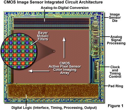
The architecture of a typical CMOS image sensor is presented in Figure 1 for an integrated circuit die that contains an active image area of 640 × 480 pixels. The photodiode array, located in the large reddish-brown central area of the chip, is blanketed by an ordered thin layer of red, green, and blue-dyed polymeric filters, each sized to fit over an individual photodiode (in a manner similar to the technology utilized for color CCDs). In order to concentrate incident photons into the photodiode electron collection wells, the filtered photodiodes are also housed beneath a miniature positive meniscus lens (see Figures 2, 3, and 4) known as a microlens, or lenticular, array. The inset in Figure 1 reveals a high magnification view of the filters and microlens array. Also included on the integrated circuit illustrated in Figure 1 is analog signal processing circuitry that collects and interprets signals generated by the photodiode array. These signals are then sent to the analog-to-digital conversion circuits, located adjacent to the photodiode array on the upper portion of the chip (as illustrated in Figure 1). Among the other duties performed by the CMOS image sensor are clock timing for the stepwise charge generation, voltage collection, transfer, and measurement duties, as well as image processing and output of the accumulated signals.
In optical microscopy, light gathered by the objective is focused by a projection lens onto the sensor surface containing a two-dimensional array of identical photodiodes, termed picture elements or pixels. Thus, array size and pixel dimensions determine the spatial resolution of the sensor. CMOS and CCD integrated circuits are inherently monochromatic (black and white) devices, responding only to the total number of electrons accumulated in the photodiodes, not to the color of light giving rise to their release from the silicon substrate. Color is detected either by passing the incident light through a sequential series of red, green, and blue filters, or with miniature transparent polymeric thin-film filters that are deposited in a mosaic pattern over the pixel array.
Solid imaging begins by determining what is signal (the useful information) versus noise (the irrelevant, confusing information) in the image and using techniques to highlight the former by creating contrast.
The first step involves looking at the part to determine how light interacts with the surface. Is it specular, matte, absorptive, refractive, or a little of everything? Reflective parts such as polished metal will reflect the light at the same angle as the light coming at the object. Matte parts will take light and scatter it all different directions. Some parts have material that will absorb light, such as ink on paper. Glass or liquid objects can change the direction of the light (refraction). Most objects have more than one of these properties. Technicians can take advantage of these differences by setting the light to highlight specific features of interest as part of an automated inspection or sortation system. In short, they can choose to highlight the signal and minimize the noise in any given image.
The arrival of high-resolution solid state imaging devices, primarily charge-coupled devices (CCDs) and complementary metal oxide semiconductor (CMOS) image sensors, has heralded a new era for optical microscopy that threatens to eclipse traditional image recording technology, such as film, video tubes, and photomultipliers. Charge-coupled device camera systems designed specifically for microscopy applications are offered by numerous original equipment and aftermarket manufacturers, and CMOS imaging sensors are now becoming available for a few microscopes.
The next step in the sequence is image recovery (see Figure 7) and the application of fundamental algorithms necessary to prepare the final image for display encoding. Nearest neighbor interpolation is performed on the pixels, which are then filtered with anti-aliasing algorithms and scaled. Additional image processing steps in the recovery engine often include anti-vignetting, spatial distortion correction, white and black balancing, smoothing, sharpening, color balance, aperture correction, and gamma adjustment. In some cases, CMOS image sensors are equipped with auxiliary circuits that enable on-chip features such as anti-jitter (image stabilization) and image compression. When the image has been sufficiently processed, it is sent to a digital signal processor for buffering to an output port.
Bright fieldvsdark fieldvsphase contrast
A question often arises as to the exact nature of color reproduction and spatial resolution from photodiode arrays having pixels divided into the basic elements of the Bayer filter pattern. A photodiode array having pixel dimensions of 640 × 480 pixels contains a total of 307,200 pixels, which yields 76,800 Bayer quartets. Does this mean that the actual useful image spatial resolution is reduced to 320 × 240 pixels? Fortunately, spatial resolution is primarily determined by the luminance component of color images and not the chrominance (color) component. This occurs because the human brain enables rather coarse color information to be added to fine spatial information and integrates the two almost seamlessly. In addition, the Bayer filters have broad wavelength transmission bands (see Figure 4) with large regions of overlap, which allows spatial information from other spectral regions to pass through the filters rendering each color with a considerable degree of spatial information.
Also illustrated in Figure 2(b) is a small portion of the microlens array (also termed lenslets) deposited by photolithography onto the surface of the Bayer filters and aligned so that each lens overlies an individual filter. The shape of the miniature lens elements approaches that of a convex meniscus lens and serves to focus incident light directly into the photosensitive area of the photodiode. Beneath the Bayer filter and microlens arrays are the photodiodes themselves, which are illustrated in Figure 2(c) as four complete photodiode assemblies or pixel units. One of the photodiodes in Figure 2(c) is identified with a large white box (upper right-hand corner) that also contains a smaller rectangular box within the larger grid. The white boxes are identified with the letters P and T, which refer to the photon collection (photosensitive) and support transistor areas of the pixel, respectively.
Both technologies were developed between the early and late 1970s, but CMOS sensors had unacceptable performance and were generally overlooked or considered just a curiosity until the early 1990s. By that time, advances in CMOS design were yielding chips with smaller pixel sizes, reduced noise, more capable image processing algorithms, and larger imaging arrays. Among the major advantages enjoyed by CMOS sensors are their low power consumption, master clock, and single-voltage power supply, unlike CCDs that often require 5 or more supply voltages at different clock speeds with significantly higher power consumption. Both CMOS and CCD chips sense light through similar mechanisms, by taking advantage of the photoelectric effect, which occurs when photons interact with crystallized silicon to promote electrons from the valence band into the conduction band. Note that the term "CMOS" refers to the process by which the image sensor is manufactured and not to a specific imaging technology.
As is evident from examining the photodiode elements in Figure 2(c), a majority of the pixel (approximately 70 percent in this example) area is dedicated to the support transistors (amplifier, reset, and row select), which are relatively opaque to visible light photons and cannot be utilized for photon detection. The remaining 30 percent (the smaller white box labeled P in Figure 2(c)) represents the photosensitive part of the pixel. Because such a small portion of the photodiode is actually capable of absorbing photons to generate charge, the fill factor or aperture of the CMOS chip and photodiodes illustrated in Figures 1, 2, and 3 represents only 30 percent of the total photodiode array surface area. The consequence is a significant loss in sensitivity and a corresponding reduction in signal-to-noise ratio, leading to a limited dynamic range. Fill factor ratios vary from device to device, but in general, they range from 30 to 80 percent of the pixel area in CMOS sensors.


 Ms.Cici
 8618319014500