
Theatrical Lighting - Lighting Fixtures - Fresnels - fresnel lights
High Luminance Uniform Lighting Sidelit No Flickering No Spot Offices LED Panel Lights Customized Size 600*1200mm 75W, Find Details about LED Panel Light, ...
F Vatansever · 2012 · 405 — Far infrared (FIR) radiation (λ = 3–100 μm) is a subdivision of the electromagnetic spectrum that has been investigated for biological effects.
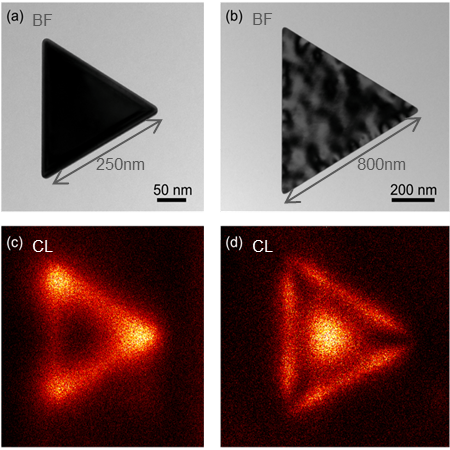
Research in nanoparticles is poised to revolutionize the fields of medicine, electronics, and energy. Optical applications relate to several classes of nanoparticles, such as quantum dots, plasmonic nanoparticles, and semiconductor nanowires. Due to their size, it can be difficult to characterize the optical properties of these nanostructures at the individual particle and sub-particle level. However, cathodoluminescence provides a direct characterization technique that allows access to the optical/electronic properties and the fundamental physics underlying individual nanoparticles. As demonstrated here, you can resolve plasmonic particles (in this example, gold triangular prisms) that vary in size to determine how the electrons in the prism are oscillating at different resonances.
Cool earnings in Vavada affiliate programme. Become a Vavada Casino affiliate today to earn up to 0 per referred customer on the fast model, as well as earn up to 50% on long-term Revshare partnerships.
Validate new growth processes when you reveal stacking fault distribution in non-polar materials with spectrally resolved imaging using low vibration cryogenic cooling stages.
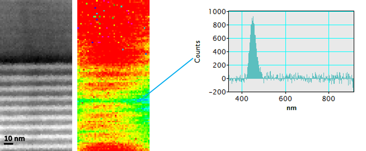
LEDs offer a variety of benefits over conventional light sources (e.g., incandescent bulbs) because they are based on semiconducting materials that deliver greatly enhanced energy efficiency and lifetime. Fast atomic EELS has proven to be a useful way to analyze GaN/InGaN multilayers within these devices. As seen here, atomic maps (right) that correlate with an annular dark field (ADF) STEM survey image (left) show how you can differentiate between layers; specifically Ga L map (top), In M map (middle), and N K map (bottom).
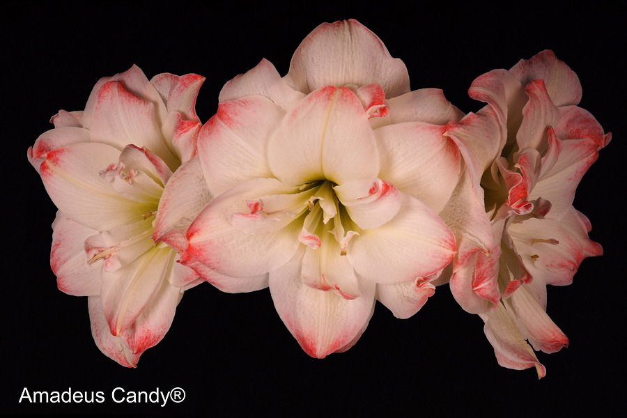
The large amaryllis Spotlight® brightens up any space. This striking amaryllis has lovely, large flowers with broad white and pink petals. The heart of the flower is apple green and each petal has beautiful red markings along its edges. This delightful large amaryllis looks great in any home! Spotlight is easy to care for and is guaranteed to bloom.Buy your Spotlight amaryllis now online.
The ability to resolve complex structures and detect material variances is important to being able to scale materials for a production environment. Using unfiltered CL imaging in the SEM, variations in cathodoluminescence were used to highlight the complex structure of boron nitride. This was followed with a high-resolution spectral analysis in deep UV of the near band edge emission (200 – 230 nm) to further understand the material’s composition.
CdS/CdTe quantum dots are used in the red pixels of Sony Bravia televisions. While quantum dots are a good source of light, individual quantum dots will radiate light to different degrees. Here you can see the first measurement to reveal the large differences in quantum efficiency when the cathodoluminescence image (red) overlaid onto the regular black and white TEM image. Courtesy of After G. Fern et al., Journal SID.
While light emitting technologies are widely available, there is demand for next generation materials to deliver a higher performance in terms of brightness, efficacy and color accuracy. As researchers continue to make substantial strides to improve the performance of light emitting devices and nanoparticles, the relationship between microstructure, defects and the optical properties of materials becomes increasingly important. The ability to calculate optical responses is crucial to understand, employ and predict failures in new materials, surfaces and interfaces, nanostructures, clusters, and materials under various extreme conditions. Useful information to characterize these features (e.g., quantum well structure) in the nanoscale size regime include:
The large amaryllis Spotlight® brightens up any space. This striking amaryllis has lovely, large flowers with broad white and pink petals. The heart of the flower is apple green and each petal has beautiful red markings along its edges. This delightful large amaryllis looks great in any home! Spotlight is easy to care for and is guaranteed to bloom.Buy your Spotlight amaryllis now online.
Carson Optical MagniFlip Flip-Open Handheld Magnifiers (CSNGN33) Item: 23978985 Model: CSNGN33 8 Price is $9.59
Luminescence spectra from individual quantum wells in an LED is shown with the first direct evidence for mitigation of the quantum confined Stark effect by silicon doping quantum barriers. Spectral line scan across LED multi-quantum well structure of a commercial LED with high Si in quantum barriers. Courtesy J. Griffiths et al., Nano Letters.
Photons falling onto a semiconductor material can be divided into three groups based on their energy compared to that of the semiconductor band gap.
2023711 — Magnification: Your microscope has 4 objective lenses: Scanning (4x), Low (10x), High (40x), and Oil Immersion (100x). In this lab, you will ...
As you can see here, this semiconductor nanorod is made of alternating InGaN (bright) and AlN (dark) layers. Using the Vulcan™ detector, you can clearly distinguish the cathodoluminescence emission from each quantum well overlaid on the high-angle annular dark field (HAADF) image. Spectra extracted from the quantum well show a change in intensity and emission wavelength that correspond with the effective band gap in nanometer spatial resolution. Courtesy of Dr. R. Williams, Ohio State University.
The large Spotlight amaryllis has colorful large flowers with a diameter of about 16 centimeters. The stem of Spotlight is about 55 centimeters long and the flower bulb has a diameter of about 9 centimeters.Plant the amaryllis flower bulb in the flowerpot of your choice and place the pot in a light and warm place. Spotlight blooms after about 8 weeks.
Other common colors of the spectrum, in order of decreasing wavelength, may be remembered by the mnemonic: ROY G BIV. The wavelengths of what we perceive as ...
UV Black Light,Flood Light with Plug 6W LED,Neon Glow for Glow Party,Halloween, Fluorescent Poster,Body Paint, Aquarium,Glow in The Dark(for Indoor use)… Add.
UV Resin Kit with Light, 50G UV Glue Kit for Bonding UV Resin with UV Flashlight ... UV Light 50ml UV Glue UV Curing Adhesive Transparent Acrylic Glue Glass ...
Correlate microstructure of individual InGaN quantum wells with luminescence to evaluate the structure of a blue LED. These results are important because the HREM image (left) is not sufficient to analyze the functional properties across multiple quantum wells. However, the cathodoluminescence image (right) acquired with the Vulcan detector shows that you can resolve individual quantum wells then characterize their luminescence intensity, then correlate to the individual well composition using spectral analysis. There is literally no other technique that can do this. Sample courtesy of J. Griffiths, University of Cambridge.
Dislocation density is a simple but important measurement to determine the validity of a grown material. During semiconductor development, dislocations can reduce device efficiency, but even more importantly cause lifetime issues associated with high leakage currents that may grow to become catastrophic defects. Unfiltered CL imaging in the SEM is proven to be a contactless, non-destructive means to quantify electrically active dislocations (revealed as dark spots in a CL image) and determine validity of a given device (e.g., less than 1 x 108 cm-2 indicates a nitride semiconductor is good).
Plane polarised light is made up of waves with the same direction of vibration for all of them. Light can be polarised through reflection or passing through ...
Categories. LED Lighting(477). Tube Lights and Crossfade Lamps(31). Tungsten Lighting(27). HMI/Daylight Lighting(24). China Balls(19). Show more ; Brands.
To adequately characterize and understand light emitting devices and nanoparticles, you must first ensure each specimen is of the highest quality to resolve the material interface and properly controlled so you manipulate it, when necessary, under environmental stimuli. Once prepared, several techniques are available to better understand the relationship between microstructure, defects and the optical properties of materials.


 Ms.Cici
 8618319014500