
Ring Lights for Content Creators - JOBY - ring lighting
Lateralillumination
"This demonstrates there are no fundamental show-stoppers in fabricating devices using extreme ultraviolet lithography," said Richard Stulen, who manages Sandia's Advanced Electronics Manufacturing Technologies Department in which the work takes place. "It's the world's first proof of principle for device fabrication with EUVL." Results of the Sandia project were presented Thursday in Boston at a meeting of the Optical Society of America by project leader Khanh Nguyen. Nguyen first demonstrated the device's operation on April 13 by examining its electrical characteristics using equipment at the University of California at Berkeley's Electrical Engineering Department. Additional highlights from the EUV lithography program were given by Sandia and Lawrence Livermore National Laboratory collaborators at the meeting, significantly increasing confidence in the feasibility of this advanced lithography tool. Current leading edge chip patterns are printed with a photographic-like process, optical lithography, creating features that are 0.35 micron wide. However, optical lithography is reaching physical limits. The shorter wavelengths of extreme ultraviolet light enable printing smaller features at high resolution. The experimental lithography tool assembled at Sandia a year ago is the first extreme ultraviolet patterning system capable of overlaying features, a precise and demanding function which is necessary to create a working device. Lithography has been targeted as a key technology for semiconductors as they continue to be made smaller, faster and more powerful. The Semiconductor Industry Association aims for commercial production of microchips with 0.1 micron features in the year 2007. The Sandia project is sponsored by the Department of Energy's Technology Transfer Initiative program in collaboration with LLNL, AT&T Bell Labs, Intel and other partners. As the project proceeds, the researchers will create more complicated devices and circuits to evaluate and develop the fabrication processes further, Stulen said. Sandia National Laboratories is a multiprogram Department of Energy laboratory, operated by a subsidiary of Lockheed Martin Corp. With main facilities located in Albuquerque, N.M., and Livermore, Calif., Sandia has major research and development responsibilities in national defense, energy, environmental technologies and economic competitiveness. Sandia is a multiprogram laboratory operated by Sandia Corporation, a Lockheed Martin Company, for the United States Department of Energy. Media contact:Nancy Garcia, Nancy_Garcia@Sandia.gov (510) 294-2932 Technical contact:Richard Stulen, (510) 294-2070 Khanh Nguyen, (510) 294-2218
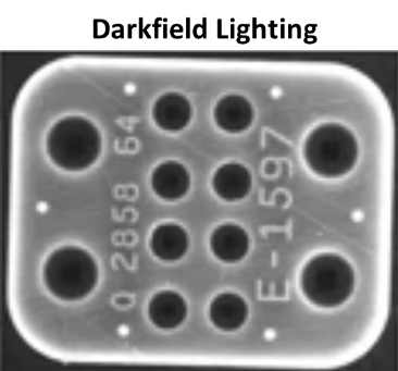
The images below, (Image 8A) and (Image 8B), were used for an application that requires counting the pins of a connector. As you can see, the bright field lighting on the left does not produce a clear image, but the dark field lighting on the right does.
This example (Image 10A), (Image 10B), and (Image 10C) highlight different lighting techniques on the same object. In the (Image 10A) image, backlighting is used to measure the smaller hole diameter. In the image (Image 10B), dome lighting is used to inspect the upper hole's taper in reference to the lower hole. In (Image 10C) dark field lighting is used for optical character recognition “OCR” on the object. Each of these could be viewed as positive or negative, depending on your goal.
Lithography has been targeted as a key technology for semiconductors as they continue to be made smaller, faster and more powerful. The Semiconductor Industry Association aims for commercial production of microchips with 0.1 micron features in the year 2007. The Sandia project is sponsored by the Department of Energy's Technology Transfer Initiative program in collaboration with LLNL, AT&T Bell Labs, Intel and other partners. As the project proceeds, the researchers will create more complicated devices and circuits to evaluate and develop the fabrication processes further, Stulen said. Sandia National Laboratories is a multiprogram Department of Energy laboratory, operated by a subsidiary of Lockheed Martin Corp. With main facilities located in Albuquerque, N.M., and Livermore, Calif., Sandia has major research and development responsibilities in national defense, energy, environmental technologies and economic competitiveness. Sandia is a multiprogram laboratory operated by Sandia Corporation, a Lockheed Martin Company, for the United States Department of Energy. Media contact:Nancy Garcia, Nancy_Garcia@Sandia.gov (510) 294-2932 Technical contact:Richard Stulen, (510) 294-2070 Khanh Nguyen, (510) 294-2218
Advancedillumination
The Sandia project is sponsored by the Department of Energy's Technology Transfer Initiative program in collaboration with LLNL, AT&T Bell Labs, Intel and other partners. As the project proceeds, the researchers will create more complicated devices and circuits to evaluate and develop the fabrication processes further, Stulen said. Sandia National Laboratories is a multiprogram Department of Energy laboratory, operated by a subsidiary of Lockheed Martin Corp. With main facilities located in Albuquerque, N.M., and Livermore, Calif., Sandia has major research and development responsibilities in national defense, energy, environmental technologies and economic competitiveness. Sandia is a multiprogram laboratory operated by Sandia Corporation, a Lockheed Martin Company, for the United States Department of Energy. Media contact:Nancy Garcia, Nancy_Garcia@Sandia.gov (510) 294-2932 Technical contact:Richard Stulen, (510) 294-2070 Khanh Nguyen, (510) 294-2218
Smart cameras and industrial cameras and the two distinct approaches in machine vision that vary in solutions and price ranges
Machine visionBacklight
Dark field lighting is required to be very close to the part, usually within an inch. The mounting angle of the dark field LEDs needs to be at least 45 degrees or more to create the desired effect (Image 3A). In short, it has the opposite effect of Bright Field lighting, meaning the surface or field is dark, and the indentations or bumps will be much brighter (Image 3B).
Diffused dome lighting, aka the salad bowl light, works by having a hole at the top of the salad bowl where the camera is mounted and the LEDs are mounted down at the rim of the salad bowl, pointing straight up, which causes the light to reflect off of the curved surface of the salad bowl. It creates a very uniform reflection (Image 5A). Diffused dome lighting is used when the object you are inspecting is curved or non-uniform (Image 5B). After applying this lighting technique to an uneven surface or texture, hotspots, and other sharp details are deemphasized, creating a matte finish to the image (Image 5C).
In order to add a free sample product to the cart we will need to remove all the normal products from the cart. Are you sure you want to continue
Analytics and diagnostics are crucial for predictive maintenance, enhancing equipment effectiveness, and monitoring machine condition
Dome LightMachine Vision
Vision code readers provide fast read rates, detect codes from multiple directions, read multiple codes simultaneously, and store extensive information
LEDillumination
Diffused on-axis lighting, or DOAL, works by having a LED light source pointed at a beam splitter. The reflected light is then parallel with the direction in which the camera is mounted (Image 6A). DOAL lighting should only be used on flat surfaces where you are trying to diminish very shiny parts of the surface to create a uniform image. Applications like DVD, CD, or silicon wafer inspection are some of the most common uses for this type of lighting.
Backlighting works by having the camera pointed directly at the backlight in a perpendicular mount. The object you are inspecting is positioned between the camera and the backlight (Image 4A). This lighting technique is the most robust because it creates a black target on a white background (Image 4B).
Additional highlights from the EUV lithography program were given by Sandia and Lawrence Livermore National Laboratory collaborators at the meeting, significantly increasing confidence in the feasibility of this advanced lithography tool. Current leading edge chip patterns are printed with a photographic-like process, optical lithography, creating features that are 0.35 micron wide. However, optical lithography is reaching physical limits. The shorter wavelengths of extreme ultraviolet light enable printing smaller features at high resolution. The experimental lithography tool assembled at Sandia a year ago is the first extreme ultraviolet patterning system capable of overlaying features, a precise and demanding function which is necessary to create a working device. Lithography has been targeted as a key technology for semiconductors as they continue to be made smaller, faster and more powerful. The Semiconductor Industry Association aims for commercial production of microchips with 0.1 micron features in the year 2007. The Sandia project is sponsored by the Department of Energy's Technology Transfer Initiative program in collaboration with LLNL, AT&T Bell Labs, Intel and other partners. As the project proceeds, the researchers will create more complicated devices and circuits to evaluate and develop the fabrication processes further, Stulen said. Sandia National Laboratories is a multiprogram Department of Energy laboratory, operated by a subsidiary of Lockheed Martin Corp. With main facilities located in Albuquerque, N.M., and Livermore, Calif., Sandia has major research and development responsibilities in national defense, energy, environmental technologies and economic competitiveness. Sandia is a multiprogram laboratory operated by Sandia Corporation, a Lockheed Martin Company, for the United States Department of Energy. Media contact:Nancy Garcia, Nancy_Garcia@Sandia.gov (510) 294-2932 Technical contact:Richard Stulen, (510) 294-2070 Khanh Nguyen, (510) 294-2218
Structured laser line lighting works by projecting a laser line onto a three-dimensional object (Image 7A), resulting in an image that gives information on the object's height. Depending on the mounting angle of the camera and laser line transmitter, the resulting laser line shift will be larger or smaller as you change the angle of the devices (Image 7B). When there is no object, the laser line will be flat (Image 7C).
What isilluminationof light
Illuminationtechniques in slit lamp
The device is a field effect transistor, a common building block of all integrated circuits. It has an electrical channel, or gate width of 0.10 microns - a thousandth the width of a human hair - more than three times smaller than devices on current chips. "This demonstrates there are no fundamental show-stoppers in fabricating devices using extreme ultraviolet lithography," said Richard Stulen, who manages Sandia's Advanced Electronics Manufacturing Technologies Department in which the work takes place. "It's the world's first proof of principle for device fabrication with EUVL." Results of the Sandia project were presented Thursday in Boston at a meeting of the Optical Society of America by project leader Khanh Nguyen. Nguyen first demonstrated the device's operation on April 13 by examining its electrical characteristics using equipment at the University of California at Berkeley's Electrical Engineering Department. Additional highlights from the EUV lithography program were given by Sandia and Lawrence Livermore National Laboratory collaborators at the meeting, significantly increasing confidence in the feasibility of this advanced lithography tool. Current leading edge chip patterns are printed with a photographic-like process, optical lithography, creating features that are 0.35 micron wide. However, optical lithography is reaching physical limits. The shorter wavelengths of extreme ultraviolet light enable printing smaller features at high resolution. The experimental lithography tool assembled at Sandia a year ago is the first extreme ultraviolet patterning system capable of overlaying features, a precise and demanding function which is necessary to create a working device. Lithography has been targeted as a key technology for semiconductors as they continue to be made smaller, faster and more powerful. The Semiconductor Industry Association aims for commercial production of microchips with 0.1 micron features in the year 2007. The Sandia project is sponsored by the Department of Energy's Technology Transfer Initiative program in collaboration with LLNL, AT&T Bell Labs, Intel and other partners. As the project proceeds, the researchers will create more complicated devices and circuits to evaluate and develop the fabrication processes further, Stulen said. Sandia National Laboratories is a multiprogram Department of Energy laboratory, operated by a subsidiary of Lockheed Martin Corp. With main facilities located in Albuquerque, N.M., and Livermore, Calif., Sandia has major research and development responsibilities in national defense, energy, environmental technologies and economic competitiveness. Sandia is a multiprogram laboratory operated by Sandia Corporation, a Lockheed Martin Company, for the United States Department of Energy. Media contact:Nancy Garcia, Nancy_Garcia@Sandia.gov (510) 294-2932 Technical contact:Richard Stulen, (510) 294-2070 Khanh Nguyen, (510) 294-2218
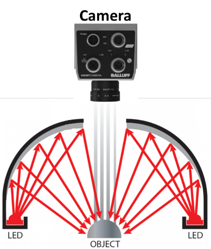
The key to deploying a robust machine vision application in a factory automation setting is ensuring you create the environment for a stable image. The three areas you must focus on to ensure image stability are lighting, lensing, and material handling. For this blog, I will focus on the seven main lighting techniques used in machine vision applications.
Sandia National Laboratories is a multiprogram Department of Energy laboratory, operated by a subsidiary of Lockheed Martin Corp. With main facilities located in Albuquerque, N.M., and Livermore, Calif., Sandia has major research and development responsibilities in national defense, energy, environmental technologies and economic competitiveness. Sandia is a multiprogram laboratory operated by Sandia Corporation, a Lockheed Martin Company, for the United States Department of Energy. Media contact:Nancy Garcia, Nancy_Garcia@Sandia.gov (510) 294-2932 Technical contact:Richard Stulen, (510) 294-2070 Khanh Nguyen, (510) 294-2218
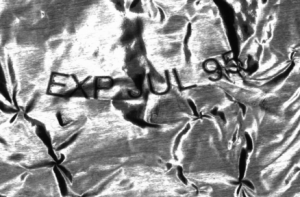
This next example (Image 9A) and (Image 9B) was for an application requiring a bar code read through a cellophane wrapper. The unclear image (Image 9A) was acquired using an on-axis ring light, while dome lighting (Image 9B) resulted in a clear, easy-to-read image of the bar code.
Dark field lighting
LIVERMORE, Calif. -- The world's first working microelectronic device to be made with extreme ultraviolet light has been fabricated at Sandia National Laboratories/California. The device is a field effect transistor, a common building block of all integrated circuits. It has an electrical channel, or gate width of 0.10 microns - a thousandth the width of a human hair - more than three times smaller than devices on current chips. "This demonstrates there are no fundamental show-stoppers in fabricating devices using extreme ultraviolet lithography," said Richard Stulen, who manages Sandia's Advanced Electronics Manufacturing Technologies Department in which the work takes place. "It's the world's first proof of principle for device fabrication with EUVL." Results of the Sandia project were presented Thursday in Boston at a meeting of the Optical Society of America by project leader Khanh Nguyen. Nguyen first demonstrated the device's operation on April 13 by examining its electrical characteristics using equipment at the University of California at Berkeley's Electrical Engineering Department. Additional highlights from the EUV lithography program were given by Sandia and Lawrence Livermore National Laboratory collaborators at the meeting, significantly increasing confidence in the feasibility of this advanced lithography tool. Current leading edge chip patterns are printed with a photographic-like process, optical lithography, creating features that are 0.35 micron wide. However, optical lithography is reaching physical limits. The shorter wavelengths of extreme ultraviolet light enable printing smaller features at high resolution. The experimental lithography tool assembled at Sandia a year ago is the first extreme ultraviolet patterning system capable of overlaying features, a precise and demanding function which is necessary to create a working device. Lithography has been targeted as a key technology for semiconductors as they continue to be made smaller, faster and more powerful. The Semiconductor Industry Association aims for commercial production of microchips with 0.1 micron features in the year 2007. The Sandia project is sponsored by the Department of Energy's Technology Transfer Initiative program in collaboration with LLNL, AT&T Bell Labs, Intel and other partners. As the project proceeds, the researchers will create more complicated devices and circuits to evaluate and develop the fabrication processes further, Stulen said. Sandia National Laboratories is a multiprogram Department of Energy laboratory, operated by a subsidiary of Lockheed Martin Corp. With main facilities located in Albuquerque, N.M., and Livermore, Calif., Sandia has major research and development responsibilities in national defense, energy, environmental technologies and economic competitiveness. Sandia is a multiprogram laboratory operated by Sandia Corporation, a Lockheed Martin Company, for the United States Department of Energy. Media contact:Nancy Garcia, Nancy_Garcia@Sandia.gov (510) 294-2932 Technical contact:Richard Stulen, (510) 294-2070 Khanh Nguyen, (510) 294-2218
Off-axis bright field lighting works by having a separate LED source mounted at about 15 degrees off perpendicular and having the camera mounted perpendicular to the surface (Image 2A). This lighting technique works best on mostly flat surfaces. The main surface or field will be bright, and the holes or indentations will be dark (Image 2B).
On-axis ring lighting is the most common type of lighting because, in many cases, it is integrated on the camera and available as one part number. When using this type of lighting, you almost always want to be a few degrees off perpendicular (Image 1A). If you are perpendicular to the object, you will get hot spots in the image (Image 1B), which is undesirable. When the camera with its ring light is tilted slightly off perpendicular you achieve the desired image (Image 1C).
The shorter wavelengths of extreme ultraviolet light enable printing smaller features at high resolution. The experimental lithography tool assembled at Sandia a year ago is the first extreme ultraviolet patterning system capable of overlaying features, a precise and demanding function which is necessary to create a working device. Lithography has been targeted as a key technology for semiconductors as they continue to be made smaller, faster and more powerful. The Semiconductor Industry Association aims for commercial production of microchips with 0.1 micron features in the year 2007. The Sandia project is sponsored by the Department of Energy's Technology Transfer Initiative program in collaboration with LLNL, AT&T Bell Labs, Intel and other partners. As the project proceeds, the researchers will create more complicated devices and circuits to evaluate and develop the fabrication processes further, Stulen said. Sandia National Laboratories is a multiprogram Department of Energy laboratory, operated by a subsidiary of Lockheed Martin Corp. With main facilities located in Albuquerque, N.M., and Livermore, Calif., Sandia has major research and development responsibilities in national defense, energy, environmental technologies and economic competitiveness. Sandia is a multiprogram laboratory operated by Sandia Corporation, a Lockheed Martin Company, for the United States Department of Energy. Media contact:Nancy Garcia, Nancy_Garcia@Sandia.gov (510) 294-2932 Technical contact:Richard Stulen, (510) 294-2070 Khanh Nguyen, (510) 294-2218
Current leading edge chip patterns are printed with a photographic-like process, optical lithography, creating features that are 0.35 micron wide. However, optical lithography is reaching physical limits. The shorter wavelengths of extreme ultraviolet light enable printing smaller features at high resolution. The experimental lithography tool assembled at Sandia a year ago is the first extreme ultraviolet patterning system capable of overlaying features, a precise and demanding function which is necessary to create a working device. Lithography has been targeted as a key technology for semiconductors as they continue to be made smaller, faster and more powerful. The Semiconductor Industry Association aims for commercial production of microchips with 0.1 micron features in the year 2007. The Sandia project is sponsored by the Department of Energy's Technology Transfer Initiative program in collaboration with LLNL, AT&T Bell Labs, Intel and other partners. As the project proceeds, the researchers will create more complicated devices and circuits to evaluate and develop the fabrication processes further, Stulen said. Sandia National Laboratories is a multiprogram Department of Energy laboratory, operated by a subsidiary of Lockheed Martin Corp. With main facilities located in Albuquerque, N.M., and Livermore, Calif., Sandia has major research and development responsibilities in national defense, energy, environmental technologies and economic competitiveness. Sandia is a multiprogram laboratory operated by Sandia Corporation, a Lockheed Martin Company, for the United States Department of Energy. Media contact:Nancy Garcia, Nancy_Garcia@Sandia.gov (510) 294-2932 Technical contact:Richard Stulen, (510) 294-2070 Khanh Nguyen, (510) 294-2218


 Ms.Cici
 8618319014500