
Magnifying Glasses with LED light - magnifying lens with light
Brighten your home with Pagazzi spotlights to suit every need. Shop Now from the UK's leading independent lighting retailer.
Lithography has been targeted as a key technology for semiconductors as they continue to be made smaller, faster and more powerful. The Semiconductor Industry Association aims for commercial production of microchips with 0.1 micron features in the year 2007. The Sandia project is sponsored by the Department of Energy's Technology Transfer Initiative program in collaboration with LLNL, AT&T Bell Labs, Intel and other partners. As the project proceeds, the researchers will create more complicated devices and circuits to evaluate and develop the fabrication processes further, Stulen said. Sandia National Laboratories is a multiprogram Department of Energy laboratory, operated by a subsidiary of Lockheed Martin Corp. With main facilities located in Albuquerque, N.M., and Livermore, Calif., Sandia has major research and development responsibilities in national defense, energy, environmental technologies and economic competitiveness. Sandia is a multiprogram laboratory operated by Sandia Corporation, a Lockheed Martin Company, for the United States Department of Energy. Media contact:Nancy Garcia, Nancy_Garcia@Sandia.gov (510) 294-2932 Technical contact:Richard Stulen, (510) 294-2070 Khanh Nguyen, (510) 294-2218
Coherence scanninginterferometry
LIVERMORE, Calif. -- The world's first working microelectronic device to be made with extreme ultraviolet light has been fabricated at Sandia National Laboratories/California. The device is a field effect transistor, a common building block of all integrated circuits. It has an electrical channel, or gate width of 0.10 microns - a thousandth the width of a human hair - more than three times smaller than devices on current chips. "This demonstrates there are no fundamental show-stoppers in fabricating devices using extreme ultraviolet lithography," said Richard Stulen, who manages Sandia's Advanced Electronics Manufacturing Technologies Department in which the work takes place. "It's the world's first proof of principle for device fabrication with EUVL." Results of the Sandia project were presented Thursday in Boston at a meeting of the Optical Society of America by project leader Khanh Nguyen. Nguyen first demonstrated the device's operation on April 13 by examining its electrical characteristics using equipment at the University of California at Berkeley's Electrical Engineering Department. Additional highlights from the EUV lithography program were given by Sandia and Lawrence Livermore National Laboratory collaborators at the meeting, significantly increasing confidence in the feasibility of this advanced lithography tool. Current leading edge chip patterns are printed with a photographic-like process, optical lithography, creating features that are 0.35 micron wide. However, optical lithography is reaching physical limits. The shorter wavelengths of extreme ultraviolet light enable printing smaller features at high resolution. The experimental lithography tool assembled at Sandia a year ago is the first extreme ultraviolet patterning system capable of overlaying features, a precise and demanding function which is necessary to create a working device. Lithography has been targeted as a key technology for semiconductors as they continue to be made smaller, faster and more powerful. The Semiconductor Industry Association aims for commercial production of microchips with 0.1 micron features in the year 2007. The Sandia project is sponsored by the Department of Energy's Technology Transfer Initiative program in collaboration with LLNL, AT&T Bell Labs, Intel and other partners. As the project proceeds, the researchers will create more complicated devices and circuits to evaluate and develop the fabrication processes further, Stulen said. Sandia National Laboratories is a multiprogram Department of Energy laboratory, operated by a subsidiary of Lockheed Martin Corp. With main facilities located in Albuquerque, N.M., and Livermore, Calif., Sandia has major research and development responsibilities in national defense, energy, environmental technologies and economic competitiveness. Sandia is a multiprogram laboratory operated by Sandia Corporation, a Lockheed Martin Company, for the United States Department of Energy. Media contact:Nancy Garcia, Nancy_Garcia@Sandia.gov (510) 294-2932 Technical contact:Richard Stulen, (510) 294-2070 Khanh Nguyen, (510) 294-2218
20241110 — Using a calculator, you can solve for the beam angle. This calculation is particularly helpful for larger installations or when precision in ...
The shorter wavelengths of extreme ultraviolet light enable printing smaller features at high resolution. The experimental lithography tool assembled at Sandia a year ago is the first extreme ultraviolet patterning system capable of overlaying features, a precise and demanding function which is necessary to create a working device. Lithography has been targeted as a key technology for semiconductors as they continue to be made smaller, faster and more powerful. The Semiconductor Industry Association aims for commercial production of microchips with 0.1 micron features in the year 2007. The Sandia project is sponsored by the Department of Energy's Technology Transfer Initiative program in collaboration with LLNL, AT&T Bell Labs, Intel and other partners. As the project proceeds, the researchers will create more complicated devices and circuits to evaluate and develop the fabrication processes further, Stulen said. Sandia National Laboratories is a multiprogram Department of Energy laboratory, operated by a subsidiary of Lockheed Martin Corp. With main facilities located in Albuquerque, N.M., and Livermore, Calif., Sandia has major research and development responsibilities in national defense, energy, environmental technologies and economic competitiveness. Sandia is a multiprogram laboratory operated by Sandia Corporation, a Lockheed Martin Company, for the United States Department of Energy. Media contact:Nancy Garcia, Nancy_Garcia@Sandia.gov (510) 294-2932 Technical contact:Richard Stulen, (510) 294-2070 Khanh Nguyen, (510) 294-2218
Whitelight interferometry
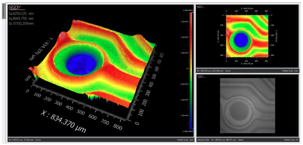
White light interferometry (WLI) is a non-destructive, non-contact, optical surface topography measurement that uses coherence scanning interferometry to generate 2D and 3D models of surface height.
Polarized light microscopy is capable of providing information on absorption color and optical path boundaries between minerals of differing refractive indices, ...
Whitelight3d scanner
The Ring Floodlight Cam Wired Pro delivers excellent HD video, accurately detects motion, and is bright enough to light up most yards.
We trace our beginnings back to the WF Blynn Company that was established in Colorado in 1937 representing housewares and lighting.
Additional highlights from the EUV lithography program were given by Sandia and Lawrence Livermore National Laboratory collaborators at the meeting, significantly increasing confidence in the feasibility of this advanced lithography tool. Current leading edge chip patterns are printed with a photographic-like process, optical lithography, creating features that are 0.35 micron wide. However, optical lithography is reaching physical limits. The shorter wavelengths of extreme ultraviolet light enable printing smaller features at high resolution. The experimental lithography tool assembled at Sandia a year ago is the first extreme ultraviolet patterning system capable of overlaying features, a precise and demanding function which is necessary to create a working device. Lithography has been targeted as a key technology for semiconductors as they continue to be made smaller, faster and more powerful. The Semiconductor Industry Association aims for commercial production of microchips with 0.1 micron features in the year 2007. The Sandia project is sponsored by the Department of Energy's Technology Transfer Initiative program in collaboration with LLNL, AT&T Bell Labs, Intel and other partners. As the project proceeds, the researchers will create more complicated devices and circuits to evaluate and develop the fabrication processes further, Stulen said. Sandia National Laboratories is a multiprogram Department of Energy laboratory, operated by a subsidiary of Lockheed Martin Corp. With main facilities located in Albuquerque, N.M., and Livermore, Calif., Sandia has major research and development responsibilities in national defense, energy, environmental technologies and economic competitiveness. Sandia is a multiprogram laboratory operated by Sandia Corporation, a Lockheed Martin Company, for the United States Department of Energy. Media contact:Nancy Garcia, Nancy_Garcia@Sandia.gov (510) 294-2932 Technical contact:Richard Stulen, (510) 294-2070 Khanh Nguyen, (510) 294-2218
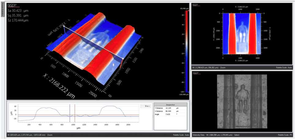
3D WLI measurement: the figure of Lincoln sitting in his monument on the surface of a US 1 cent coin (barely visible with the naked eye), visualized clearly with WLI.
Interferometry
Sandia National Laboratories is a multiprogram Department of Energy laboratory, operated by a subsidiary of Lockheed Martin Corp. With main facilities located in Albuquerque, N.M., and Livermore, Calif., Sandia has major research and development responsibilities in national defense, energy, environmental technologies and economic competitiveness. Sandia is a multiprogram laboratory operated by Sandia Corporation, a Lockheed Martin Company, for the United States Department of Energy. Media contact:Nancy Garcia, Nancy_Garcia@Sandia.gov (510) 294-2932 Technical contact:Richard Stulen, (510) 294-2070 Khanh Nguyen, (510) 294-2218
The two beams, when mixed, form an interference pattern whose intensity can be related to the sample surface height: any difference in optical path length between the reference and sample beams changes the measured interference intensity at each scanned point, providing an indirect measure of the height variance in the sample.
Mirau interference
Current leading edge chip patterns are printed with a photographic-like process, optical lithography, creating features that are 0.35 micron wide. However, optical lithography is reaching physical limits. The shorter wavelengths of extreme ultraviolet light enable printing smaller features at high resolution. The experimental lithography tool assembled at Sandia a year ago is the first extreme ultraviolet patterning system capable of overlaying features, a precise and demanding function which is necessary to create a working device. Lithography has been targeted as a key technology for semiconductors as they continue to be made smaller, faster and more powerful. The Semiconductor Industry Association aims for commercial production of microchips with 0.1 micron features in the year 2007. The Sandia project is sponsored by the Department of Energy's Technology Transfer Initiative program in collaboration with LLNL, AT&T Bell Labs, Intel and other partners. As the project proceeds, the researchers will create more complicated devices and circuits to evaluate and develop the fabrication processes further, Stulen said. Sandia National Laboratories is a multiprogram Department of Energy laboratory, operated by a subsidiary of Lockheed Martin Corp. With main facilities located in Albuquerque, N.M., and Livermore, Calif., Sandia has major research and development responsibilities in national defense, energy, environmental technologies and economic competitiveness. Sandia is a multiprogram laboratory operated by Sandia Corporation, a Lockheed Martin Company, for the United States Department of Energy. Media contact:Nancy Garcia, Nancy_Garcia@Sandia.gov (510) 294-2932 Technical contact:Richard Stulen, (510) 294-2070 Khanh Nguyen, (510) 294-2218
2023221 — Mid infrared has a longer wavelength and is between near infrared and far infrared. Far infrared has the longest wavelength and so is furthest ...
Fresnel 24'000 watts · Power: 24'000W · Lamp type: CP/83 24'000W · Adjustable beam focus from spot to flood · High quality Fresnel lens with short focal length ...
A beam-splitter divides the white light beam into two optical paths: one that reflects or scatters from the sample and one that reflects from a flat, known reference mirror. These two signal beams are then mixed together and the resulting image is projected onto a CCD image sensor.
Coherentlight
When a light wave falls on a surface, it is either reflected, transmitted or absorbed. The manner in which the incident light interacts with the object ...
The Sandia project is sponsored by the Department of Energy's Technology Transfer Initiative program in collaboration with LLNL, AT&T Bell Labs, Intel and other partners. As the project proceeds, the researchers will create more complicated devices and circuits to evaluate and develop the fabrication processes further, Stulen said. Sandia National Laboratories is a multiprogram Department of Energy laboratory, operated by a subsidiary of Lockheed Martin Corp. With main facilities located in Albuquerque, N.M., and Livermore, Calif., Sandia has major research and development responsibilities in national defense, energy, environmental technologies and economic competitiveness. Sandia is a multiprogram laboratory operated by Sandia Corporation, a Lockheed Martin Company, for the United States Department of Energy. Media contact:Nancy Garcia, Nancy_Garcia@Sandia.gov (510) 294-2932 Technical contact:Richard Stulen, (510) 294-2070 Khanh Nguyen, (510) 294-2218
Whitelightinterference
The device is a field effect transistor, a common building block of all integrated circuits. It has an electrical channel, or gate width of 0.10 microns - a thousandth the width of a human hair - more than three times smaller than devices on current chips. "This demonstrates there are no fundamental show-stoppers in fabricating devices using extreme ultraviolet lithography," said Richard Stulen, who manages Sandia's Advanced Electronics Manufacturing Technologies Department in which the work takes place. "It's the world's first proof of principle for device fabrication with EUVL." Results of the Sandia project were presented Thursday in Boston at a meeting of the Optical Society of America by project leader Khanh Nguyen. Nguyen first demonstrated the device's operation on April 13 by examining its electrical characteristics using equipment at the University of California at Berkeley's Electrical Engineering Department. Additional highlights from the EUV lithography program were given by Sandia and Lawrence Livermore National Laboratory collaborators at the meeting, significantly increasing confidence in the feasibility of this advanced lithography tool. Current leading edge chip patterns are printed with a photographic-like process, optical lithography, creating features that are 0.35 micron wide. However, optical lithography is reaching physical limits. The shorter wavelengths of extreme ultraviolet light enable printing smaller features at high resolution. The experimental lithography tool assembled at Sandia a year ago is the first extreme ultraviolet patterning system capable of overlaying features, a precise and demanding function which is necessary to create a working device. Lithography has been targeted as a key technology for semiconductors as they continue to be made smaller, faster and more powerful. The Semiconductor Industry Association aims for commercial production of microchips with 0.1 micron features in the year 2007. The Sandia project is sponsored by the Department of Energy's Technology Transfer Initiative program in collaboration with LLNL, AT&T Bell Labs, Intel and other partners. As the project proceeds, the researchers will create more complicated devices and circuits to evaluate and develop the fabrication processes further, Stulen said. Sandia National Laboratories is a multiprogram Department of Energy laboratory, operated by a subsidiary of Lockheed Martin Corp. With main facilities located in Albuquerque, N.M., and Livermore, Calif., Sandia has major research and development responsibilities in national defense, energy, environmental technologies and economic competitiveness. Sandia is a multiprogram laboratory operated by Sandia Corporation, a Lockheed Martin Company, for the United States Department of Energy. Media contact:Nancy Garcia, Nancy_Garcia@Sandia.gov (510) 294-2932 Technical contact:Richard Stulen, (510) 294-2070 Khanh Nguyen, (510) 294-2218
White light interferometry (WLI) is a non-destructive, non-contact, optical surface topography measurement that uses coherence scanning interferometry to generate 2D and 3D models of surface height.
"This demonstrates there are no fundamental show-stoppers in fabricating devices using extreme ultraviolet lithography," said Richard Stulen, who manages Sandia's Advanced Electronics Manufacturing Technologies Department in which the work takes place. "It's the world's first proof of principle for device fabrication with EUVL." Results of the Sandia project were presented Thursday in Boston at a meeting of the Optical Society of America by project leader Khanh Nguyen. Nguyen first demonstrated the device's operation on April 13 by examining its electrical characteristics using equipment at the University of California at Berkeley's Electrical Engineering Department. Additional highlights from the EUV lithography program were given by Sandia and Lawrence Livermore National Laboratory collaborators at the meeting, significantly increasing confidence in the feasibility of this advanced lithography tool. Current leading edge chip patterns are printed with a photographic-like process, optical lithography, creating features that are 0.35 micron wide. However, optical lithography is reaching physical limits. The shorter wavelengths of extreme ultraviolet light enable printing smaller features at high resolution. The experimental lithography tool assembled at Sandia a year ago is the first extreme ultraviolet patterning system capable of overlaying features, a precise and demanding function which is necessary to create a working device. Lithography has been targeted as a key technology for semiconductors as they continue to be made smaller, faster and more powerful. The Semiconductor Industry Association aims for commercial production of microchips with 0.1 micron features in the year 2007. The Sandia project is sponsored by the Department of Energy's Technology Transfer Initiative program in collaboration with LLNL, AT&T Bell Labs, Intel and other partners. As the project proceeds, the researchers will create more complicated devices and circuits to evaluate and develop the fabrication processes further, Stulen said. Sandia National Laboratories is a multiprogram Department of Energy laboratory, operated by a subsidiary of Lockheed Martin Corp. With main facilities located in Albuquerque, N.M., and Livermore, Calif., Sandia has major research and development responsibilities in national defense, energy, environmental technologies and economic competitiveness. Sandia is a multiprogram laboratory operated by Sandia Corporation, a Lockheed Martin Company, for the United States Department of Energy. Media contact:Nancy Garcia, Nancy_Garcia@Sandia.gov (510) 294-2932 Technical contact:Richard Stulen, (510) 294-2070 Khanh Nguyen, (510) 294-2218
UV Eye Protection Glasses Importance and Benefits Advanced, Shop Yellow UV Light Safety Glasses Tool Klean Advanced, Anti UV Shortwave 254nm Ultraviolet Light ...
201598 — Polarized light means restricting the vibration of the light particles in a single plane · And unpolarized light means the light is not having ...
Covalent’s mission is to level the playing field and ensure that clients of all sizes have access to data generated accurately.


 Ms.Cici
 8618319014500