
Black Oak Pro Series Double Row Combo Infrared 20 ... - ir light bar
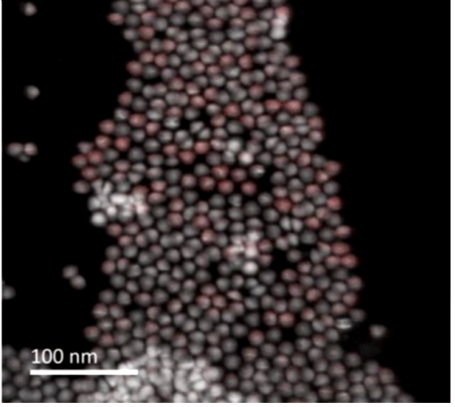
Research in nanoparticles is poised to revolutionize the fields of medicine, electronics, and energy. Optical applications relate to several classes of nanoparticles, such as quantum dots, plasmonic nanoparticles, and semiconductor nanowires. Due to their size, it can be difficult to characterize the optical properties of these nanostructures at the individual particle and sub-particle level. However, cathodoluminescence provides a direct characterization technique that allows access to the optical/electronic properties and the fundamental physics underlying individual nanoparticles. As demonstrated here, you can resolve plasmonic particles (in this example, gold triangular prisms) that vary in size to determine how the electrons in the prism are oscillating at different resonances.
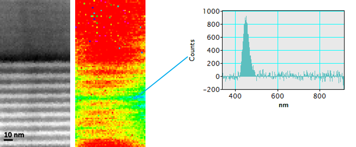
Correlate microstructure of individual InGaN quantum wells with luminescence to evaluate the structure of a blue LED. These results are important because the HREM image (left) is not sufficient to analyze the functional properties across multiple quantum wells. However, the cathodoluminescence image (right) acquired with the Vulcan detector shows that you can resolve individual quantum wells then characterize their luminescence intensity, then correlate to the individual well composition using spectral analysis. There is literally no other technique that can do this. Sample courtesy of J. Griffiths, University of Cambridge.
CdS/CdTe quantum dots are used in the red pixels of Sony Bravia televisions. While quantum dots are a good source of light, individual quantum dots will radiate light to different degrees. Here you can see the first measurement to reveal the large differences in quantum efficiency when the cathodoluminescence image (red) overlaid onto the regular black and white TEM image. Courtesy of After G. Fern et al., Journal SID.
Polarization of light is an intriguing phenomenon with a wide range of applications in diverse fields. Understanding the principles of polarization and its various states enables us to harness its potential in technologies such as polarized sunglasses, LCD displays, 3D imaging, optical communications, and material characterization. By exploring the fascinating world of polarization, we gain a deeper appreciation for the behavior of light and its practical applications in our daily lives.
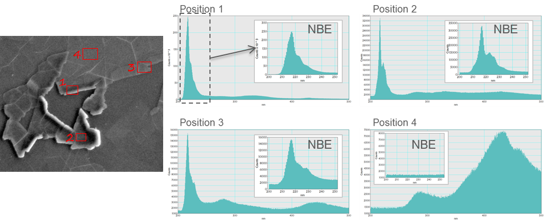
The ability to resolve complex structures and detect material variances is important to being able to scale materials for a production environment. Using unfiltered CL imaging in the SEM, variations in cathodoluminescence were used to highlight the complex structure of boron nitride. This was followed with a high-resolution spectral analysis in deep UV of the near band edge emission (200 – 230 nm) to further understand the material’s composition.
Polarization of light is a fascinating optical phenomenon that occurs when light waves oscillate in a specific orientation. This article aims to provide a comprehensive understanding of the polarization of light, including its definition, principles, polarization states, and various applications in different fields.
To adequately characterize and understand light emitting devices and nanoparticles, you must first ensure each specimen is of the highest quality to resolve the material interface and properly controlled so you manipulate it, when necessary, under environmental stimuli. Once prepared, several techniques are available to better understand the relationship between microstructure, defects and the optical properties of materials.
As you can see here, this semiconductor nanorod is made of alternating InGaN (bright) and AlN (dark) layers. Using the Vulcan™ detector, you can clearly distinguish the cathodoluminescence emission from each quantum well overlaid on the high-angle annular dark field (HAADF) image. Spectra extracted from the quantum well show a change in intensity and emission wavelength that correspond with the effective band gap in nanometer spatial resolution. Courtesy of Dr. R. Williams, Ohio State University.
Validate new growth processes when you reveal stacking fault distribution in non-polar materials with spectrally resolved imaging using low vibration cryogenic cooling stages.
While light emitting technologies are widely available, there is demand for next generation materials to deliver a higher performance in terms of brightness, efficacy and color accuracy. As researchers continue to make substantial strides to improve the performance of light emitting devices and nanoparticles, the relationship between microstructure, defects and the optical properties of materials becomes increasingly important. The ability to calculate optical responses is crucial to understand, employ and predict failures in new materials, surfaces and interfaces, nanostructures, clusters, and materials under various extreme conditions. Useful information to characterize these features (e.g., quantum well structure) in the nanoscale size regime include:
Dislocation density is a simple but important measurement to determine the validity of a grown material. During semiconductor development, dislocations can reduce device efficiency, but even more importantly cause lifetime issues associated with high leakage currents that may grow to become catastrophic defects. Unfiltered CL imaging in the SEM is proven to be a contactless, non-destructive means to quantify electrically active dislocations (revealed as dark spots in a CL image) and determine validity of a given device (e.g., less than 1 x 108 cm-2 indicates a nitride semiconductor is good).
LEDs offer a variety of benefits over conventional light sources (e.g., incandescent bulbs) because they are based on semiconducting materials that deliver greatly enhanced energy efficiency and lifetime. Fast atomic EELS has proven to be a useful way to analyze GaN/InGaN multilayers within these devices. As seen here, atomic maps (right) that correlate with an annular dark field (ADF) STEM survey image (left) show how you can differentiate between layers; specifically Ga L map (top), In M map (middle), and N K map (bottom).
Luminescence spectra from individual quantum wells in an LED is shown with the first direct evidence for mitigation of the quantum confined Stark effect by silicon doping quantum barriers. Spectral line scan across LED multi-quantum well structure of a commercial LED with high Si in quantum barriers. Courtesy J. Griffiths et al., Nano Letters.
At DoveMed, our utmost priority is your well-being. We are an online medical resource dedicated to providing you with accurate and up-to-date information on a wide range of medical topics. But we're more than just an information hub - we genuinely care about your health journey. That's why we offer a variety of products tailored for both healthcare consumers and professionals, because we believe in empowering everyone involved in the care process.Our mission is to create a user-friendly healthcare technology portal that helps you make better decisions about your overall health and well-being. We understand that navigating the complexities of healthcare can be overwhelming, so we strive to be a reliable and compassionate companion on your path to wellness.As an impartial and trusted online resource, we connect healthcare seekers, physicians, and hospitals in a marketplace that promotes a higher quality, easy-to-use healthcare experience. You can trust that our content is unbiased and impartial, as it is trusted by physicians, researchers, and university professors around the globe. Importantly, we are not influenced or owned by any pharmaceutical, medical, or media companies. At DoveMed, we are a group of passionate individuals who deeply care about improving health and wellness for people everywhere. Your well-being is at the heart of everything we do.


 Ms.Cici
 8618319014500