
Advanced illumination(美国) - advanced illumination vt
“One of the main problems we encountered when initially making these hybrids is that the inorganic content needs to be uniformly distributed inside the organic polymer while making sure that the infused inorganic components are not too strongly bound to organic matrix,” said Ashwanth Subramanian, the lead author of the paper. Subramanian is a former CFN-affiliated PhD student from Stony Brook University’s Department of Materials Science and Chemical Engineering who is now working as a process engineer at Lam Research. “It was a little difficult to achieve that in previous research. In this work, however, we were able to choose a different precursor for the metal, the inorganic source, and that allowed us to make a hybrid with a uniform composition as well as weak binding between organic and inorganic components.”
Whitelight3d scanner
7 — The Path of Light is a light art spectacle arranged by the City of Turku. It consists of a great light event and seasonal lighting on ...
Brookhaven National Laboratory is supported by the Office of Science of the U.S. Department of Energy. The Office of Science is the single largest supporter of basic research in the physical sciences in the United States and is working to address some of the most pressing challenges of our time. For more information, visit science.energy.gov.
“In our previous work, we demonstrated this concept and were working with established resist composition as a proof of concept,” explained Nikhil Tiwale, a materials scientist at CFN. “In this new paper, we used a composition that hasn’t been studied in the resist community, yielding better EUV absorption and improved patterning performance.”
“To synthesize our new hybrid resist materials, organic polymer materials are infused with inorganic metal oxides by a specialized technique known as vapor-phase infiltration. This method is one of the key areas of materials synthesis expertise at CFN. Compared to conventional chemical synthesis, we can readily generate various compositions of hybrid materials and control their material properties by infusing gaseous inorganic precursors into a solid organic matrix,” explained Chang-Yong Nam, a materials scientist at CFN who led the project.
Light reflects off of objects and enters the eyeball through a ... Lens: located directly behind the pupil, it focuses light rays onto the retina ...
Whitelightinterference
Nam’s hybrid resists show such promise that he was awarded major funding to pursue this concept through the DOE Accelerate Innovations in Emerging Technologies program. This multi-institute project will explore the development of new classes of hybrid photoresists and exploit machine learning to accelerate EUV research by making material validation easier and more accessible.
Scientists at CFN have been researching hybrid photoresist materials for several years, building a strong foundation of work culminating in the design of new, highly functional materials. Nam leads this research program with a goal of developing even more new materials and functionalities. In 2022, he was recognized as an Inventor of the Year by Battelle Memorial Institute.
The team is currently working on other hybrid material compositions and testing how they perform, as well as the processes involved in fabricating them, paving the way for patterning smaller, more efficient semiconductor devices.
Coherence scanninginterferometry
At Ebatco we offer technical expertise, state of the art instruments, market-competitive service charge rates, a quick turn around and guaranteed satisfaction! Please contact us with any questions that you may have.
The research team includes CFN staff members Kim Kisslinger, Ming Lu, and Aaron Stein, as well as Won-Il Lee, a PhD student from Stony Brook University, and Jiyoung Kim, a professor in the Department of Materials Science and Engineering at the University of Texas at Dallas. Their combined efforts have helped push EUV lithography techniques beyond current limits.
in Huntsville, AL. ... Excited about our event tonight at Inline! ... Who's ready to win a yeti?? ... Kendall Lighting Center (cont.) ... Did you know YOU can help ...
Brookhaven National Laboratory is a multipurpose research institution funded by the U.S. Department of Energy. Located on Long Island, NY, Brookhaven operates large-scale facilities for studies in physics, chemistry, biology, medicine, applied science, and advanced technology. The Laboratory's almost 3,000 scientists, engineers, and support staff are joined each year by more than 5,000 visiting researchers from around the world.
For more than 50 years, the semiconductor industry has been hard at work developing advanced technologies that have led to the amazing increases in computing power and energy efficiency that have improved our lives. A primary way the industry has achieved these remarkable performance gains has been by finding ways to decrease the size of the semiconductor devices in microchips. However, with semiconductor feature sizes now approaching only a few nanometers—just a few hundred atoms—it has become increasingly challenging to sustain continued device miniaturization.
Whitelight interferometry
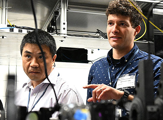
Ming Lu, Won-Il Lee, Chang-Yong Nam, Kim Kisslinger (pictured from left to right), Ashwanth Subramanian, Nikhil Tiwale, Aaron Stein, and Jiyoung Kim (not pictured) were the team members who pushed this research forward.
Mirau interference
In the case of organic photoresists, adding inorganic molecules can yield a vastly improved material for EUV. The hybrid materials have increased sensitivity to EUV light, which means that they don’t need to be exposed to as much EUV light during patterning, reducing the required process time. The hybrid materials also have improved mechanical and chemical resistance, making them better-suited as templates for high-resolution etching.
“It’s currently really hard to do EUV patterning,” explained Nam. “The actual patterning machine that industry is using is very, very expensive—the current version is more than $200 million per unit! There are only three to four companies in the world that can use it for actual chip manufacturing. There are a lot of researchers who want to study and develop new photoresist materials but can’t perform EUV patterning to evaluate them. This is one of the key challenges we hope to address.”
Dec 28, 2023 — A light meter is a tool that measures the intensity of light in a scene, helping photographers to determine the optimal combination of aperture, ...
Interferometry
In an effort to address this need, a team of scientists at the Center for Functional Nanomaterials (CFN)—a U.S. Department of Energy (DOE) Office of Science User Facility at DOE’s Brookhaven National Laboratory—has designed a new light-sensitive, organic-inorganic hybrid material that enables high-performance patternability by EUV lithography. Their results were recently published in Advanced Materials Interfaces.
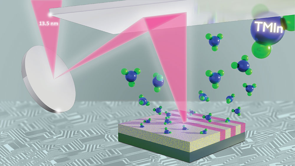
In this artist's rendition, mirrors focus extreme ultraviolet light to pattern a latent image in a polymer thin film infiltrated by indium-containing gaseous molecules.
As the team experiments and refines their materials, resists with improved performance are emerging. With any pioneering field, there are challenges to be faced.
In addition to surface roughness analysis, The Wyko NT3300 optical profilometer can also be used to acquire contour and morphology of parts in three-dimensions. Once the data is acquired, critical dimensions such as distance, depth, thickness, and other geometrical parameters can be obtained. These capabilities have found usefulness in characterizing thin films and coatings for thickness measurement through step height determination across coated and uncoated areas.
To address the challenges associated with fabricating even smaller microchip components, the semiconductor industry is currently transitioning to a more powerful fabrication method—extreme ultraviolet (EUV) lithography. EUV lithography employs light that is only 13.5 nanometers in wavelength to form tiny circuit patterns in a photoresist, the light-sensitive material integral to the lithography process. The photoresist is the template for forming the nanoscale circuit patterns in the silicon semiconductor. As EUV lithography begins paving the way for the future, scientists are faced with the hurdle of identifying the most effective resist materials for this new era of nanofabrication.
2008216 — The idea of an an optical microscope or a light microscope is to magnify images which are far too small to be seen by the naked eye.
Product Specification: Rated voltage: AC100~240V 50/60Hz; 140W@AC220V Laser: W500mW RGB LED strobe light source: single 0.2W full color × 90pcs
Coherentlight
The hybrid materials used to create these new photoresists are comprised of both organic materials—those that primarily contain carbon and oxygen atoms—and inorganic materials—those usually based on metallic elements. Both parts of the hybrid host their own unique chemical, mechanical, optical, and electrical properties due to their unique chemistry and structures. By combining these different components, new hybrid organic-inorganic materials emerge with their own interesting properties.
Blue Light Blocking Reading Glasses · Illuminated Reading Glasses ... Mobilux LED Hand-held ...
In their current research, the team noticed vast improvements after using indium as an inorganic component as compared to the aluminum that was used in the work that was done before. The scientists made the new resist using a poly(methyl methacrylate) (PMMA) organic thin film as the organic component and infiltrated it with inorganic indium oxide. This new hybrid exhibited increased sensitivity and a more uniform material makeup, which improved uniformity in subsequent patterning.
Surface roughness can tell a lot about the material something is made from and its past processing history. If the surface roughness for a part needs to be taken but making physical contact with the surface is not advised (to avoid surface damage or altering a feature of interest) than white light interferometry is a great solution. The basic principle of interferometry is that light is reflected from a reference mirror and combined with light reflected from the sample surface to produce interference fringes, where the best contrast fringe occurs at the best focus. Ebatco possesses a Wyko NT3300 white light interferometer manufactured by Veeco. The NT3300 has two measurement modes, phase shift interferometry (PSI) and vertical scanning interferometry (VSI). PSI mode uses variations in phase of a monochromatic reference light compared to light reflected off of the sample to calculate small height variations on the sample surface. This measurement mode is useful for surfaces with step-heights of less than a quarter of the wavelength used and provides sub-nanometer vertical resolution. VSI mode uses a multi-wavelength white light source to measure the degree of fringe modulation, or coherence, between the reference and sample beams. As the beam is moved vertically through the sample focus, the maximum fringe contrast is extracted at each point on the sample surface, and forms a topographical map. This mode of measurement can be used to measure features up to 2 mm in height.
Light sources are devices whose primary function is to produce visible or near-visible radiant energy for general illumination and specialty applications. They ...
When the two components are not in phase, the polarization direction rotates in time. The speed of the rotation depends on how far out of phase ...
This lux meter is useful for checking the level of luminance, the measure of the amount of light falling on a surface. It has a range of 0-50,000 lx with a ...
Brookhaven Science Associates manages and operates Brookhaven National Laboratory on behalf of the U.S. Department of Energy's Office of Science. BSA is a partnership between Battelle and The Research Foundation for the State University of New York on behalf of Stony Brook University. | More


 Ms.Cici
 8618319014500