
Liquid Line | Flexible lighting design for architects - line lighting
On axislighting
Now the light source of machine vision system mainly uses LED (light emitting diode), which is widely used in the industry due to its high degree of freedom of shape, long service life, fast response speed, good monochromaticity, various colors, and high cost performance.
3. Fast response. The response time of the LED light-emitting tube is very short. The real meaning of the response time is to ensure the operation switching between multiple light sources or between different areas of a light source. When a dedicated controller is used to supply power to the LED light source, the time to reach the maximum illumination is less than 10s.
SmartvisionLights
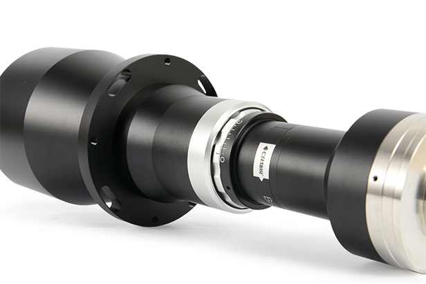
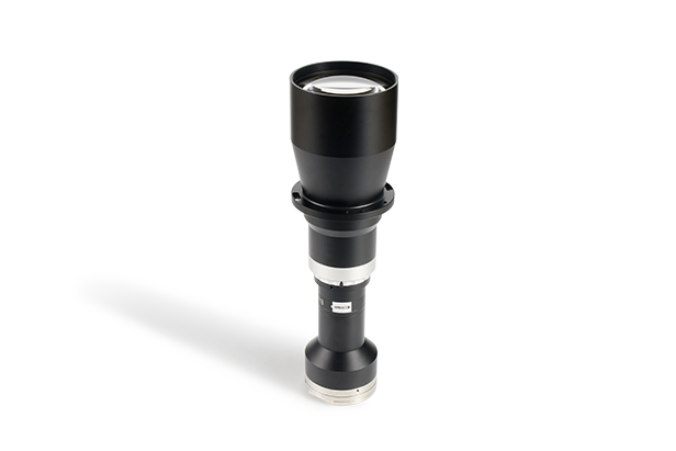
A complete machine vision inspection system includes an image collection part and an image analysis part, and the image collection part is mainly undertaken by industrial cameras, industrial lenses and machine vision light sources.
20221112 — The procedure of Dark Activated Circuit Design: So, for this circuit, 3 volts are powering the circuit. These 3 volts are in parallel to a 100KΩ ...
4. Various colors. Except for the shape of the light source. Another aspect of getting a stable image input is choosing the color of the light source. Even light sources of the same shape can produce very different images due to differences in color. In fact, how to use the technical characteristics of the color of the light source to obtain the image with the best contrast has always been the main direction of the development of the light source.
Machinevision lightingtechniques
20241015 — At Current, we are Always On and working to improve lives with the industry's most expansive portfolio of sustainable advanced lighting ...
Companies are also working on integrating autofocus functions at the wafer level. A number of players, including SEMCO, are working on electro active polymers, whose thickness can be controlled and driven electrically by applying a defined voltage. Others like Siimpel (recently acquired by Tessera) have a MEMS- based solution, using a spring-like silicon structure.
Dome Light MachineVision
These increasingly integrated optics will likely find application in other products as well, to simplify the manufacture and reduce the size and cost of other optoelectronics, across applications ranging from biomedical endoscopy to consumer products like digital cameras, pico projectors, headsup automotive displays, projection systems for gaming, and LED lighting.
A typical wafer-level optic process involves dropping a polymer layer on to a glass wafer, pressing in the desired pattern through molding and UV replication with nanoimprint lithography tools, to imprint some 4000 lenses at once on each 8-in. wafer. This wafer is then aligned and bonded to another lens or spacer wafer, then tested and finally diced into small, low-cost optical lens camera-module cubes.
2023417 — Comprising a meticulous blend of cellulose fibers, cement, and proprietary additives, this construction material is revolting the overall structural integrity ...
Illuminate the object, increase the height, form an imaging effect that is beneficial to image processing, reduce the complexity of the system and the requirements for image processing algorithms, defeat ambient light interference, ensure image stability, and improve system accuracy and power.
2023822 — I've scrounged old wall-warts and power adapters to get things like 5V, 12V, 19V, but I don't seem to have anything at 24V. Is there anything I might have ...
2. Long service life. In order for the image processing unit to obtain accurate and reproducible measurement results, the lighting machine vision system must ensure that a stable image input can be provided for a reasonably long period of time. The brightness of the LED light source decreases after 10.0 to 30,000 hours of continuous operation, but it is far better than other types of light sources. In addition, the continuous operation of the control system can suppress the heating of the luminous tube, and the service life will be doubled.
May 24, 2010 – It’s not just 3D packaging technology where CMOS image sensors are driving IC technology these days. Ultrathin silicon that enables back-side illumination (BSI), and integrated wafer-level optics are bringing sharply improved performance, lower costs, and smaller size, driving CMOS image sensors into more and more markets — and these technologies may soon impact other IC manufacturing as well.
One of the key breakthroughs that enables these major improvements in performance and price is backside illumination, which requires thinning the silicon wafer down to a transparent 5μm active layer, so the light can come in directly to the photo diode from the backside. Putting the electrical distribution layers behind the photo diode allows a simpler and more flexible BEOL architecture design, eliminating the need to leave openings in the pattern to let light through, and naturally lets in much more light, allowing higher resolution or higher sensitivity for the same given sensor size and cost. Next step, now in the development stage, is to take advantage of this increased design flexibility and add more intelligence to the system, by stacking a microprocessor DSP below the sensor — moving towards the ideal of controlling each pixel individually as in the human eye, for much improved sensor performance across different light conditions.
The next development just starting to impact the CMOS image sensor business is wafer-scale integration of the optics, to drastically reduce size and cost, and to simplify the assembly process and supply chain. The camera module unit remains one of the largest components in most cell phones, and among the most complex to manufacture, requiring sourcing and assembly of up to 15 different components, including not only lenses, but also IR filters, caps, barrels, spacers, autofocus mechanisms, and other parts. An attractive alternative is wafer-level processing of optical lenses, today already in low-volume production by Heptagon for STMicroelectronics and by Anteryon for Toshiba camera modules.
But it's so small that there isn't a universal machine vision lighting system right now. Different inspection requirements can be handled, so for each specific case, it is necessary to plan adapted lighting equipment to achieve the best effect. Improper lighting can cause many problems. Machine vision light sources are so important, they are often overlooked by many people.
Jerôme Baron tracks MEMS and advanced packaging technologies and markets at Yole Développement. He recently authored the report "CMOS Image Sensors: Technology and Markets 2010".
Easily post a comment below using your Linkedin, Twitter, Google or Facebook account. Comments won't automatically be posted to your social media accounts unless you select to share.
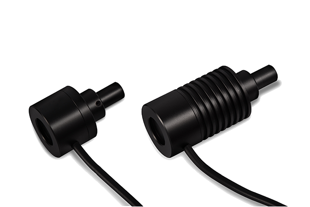
Industrial light for machine vision and image processing applications. Different sizes and colors available.
SpinCar, the global leader in digital automation trading software and data, announced today the acquisition of Georgian startup Pulsar AI.
Don't miss your chance to drastically improve your golf game with cutting-edge technology. Unleash the future of golf with our premium simulator. Perfect for: ...
Also critical is the annealing process, since this 5μm thin silicon film needs to include a very narrow implant gradient, to prevent recombination in the epi silicon and to push the photons down to the photo diodes. Since typical annealing ovens can only be controlled to about 30μm layer precision, the finer implant gradients require annealing with a nano-second, local heating laser process. The French equipment company Excico supplies a tool that uses a UV excimer type of laser source with a large spot for tight precision with better image quality and higher throughput.
The BSI process flow starts with making the photo diodes. Then the device wafer is bonded at low temperature to a silicon or glass carrier, using either adhesive polymers or molecular oxide-to-oxide bonding. US-based 3D-IC company Ziptronix offers one low-temperature bonding solution, which presses together ultraflat wafers, well prepared through specific surface preparation treatments. Next, the 1mm thick photo diode wafer is thinned down to 40-50μm with Disco or Accretech grinding tools, then thinned further with CMP, and finally etched down to an etch-stop layer at 5μm. This radical wafer thinning typically requires precise control of wet etching after initial grinding and CMP. One option, used by Sony and others, is to use SOI wafers from Soitec, using the buried oxide layer as an inner etch stop layer at the oxide interface — though the high cost of SOI wafers may limit the process to high-end imaging applications only. Others, including OmniVision, working with TSMC and Xintec, claim to have developed a lower-cost alternative process using bulk silicon wafers with graded implant layers. The trick is to find a highly selective etch chemistry that will stop precisely at the required 5μm thin silicon interface, just before reaching the photodiode structures.
For back, front and hip carry Designed to carry babies from 3.5kg to 20 kg (approx. 6 weeks to 3 years of age) Removable infant insert With seat width ...
1. Shape freedom. An LED light source is composed of many individual LEDs. Therefore, compared with other light sources, it can be made into more shapes, and it is easier to plan the shape and size of the light source according to the user's condition.
This ability to build and handle these ultrathin layers also opens new possibilities for 3D stacking and integrating very thin active layers monolithically on top of other semiconductor applications. Indeed, such type of process set-up has the potential to be re-used in the future for 3D integration of memory + memory, logic + memory or MEMS + logic applications.
SmartVisionlights Cognex
Thinning silicon wafers down to 5μm transparent films to let light through the back side is driving a 2× to 5× improvement in sensitivity for smaller pixel image sensors. Yole Développement sees CMOS sensors now moving quickly into higher performance applications, including high resolution digital SLR cameras and digital video recorders, as they come to match the performance of CCDs at lower cost. These thinning and annealing technologies may also open new possibilities for 3D stacking and integration of very thin layers of memory and logic devices in the future. Wafer-level optics are also starting to reduce camera module size and cost in even demanding handset applications, and could also bring similar improvements to projection lens systems for gaming stations and micro displays.
But the front-runner currently appears to be a potentially breakthrough technology using liquid crystal polymers. The startup LensVector plans to start production this year of a four-layer stack of 8-in. glass wafers, encapsulating liquid crystal polymers that change shape when voltage is applied to the driving electrodes — all in less than 500μm total thickness. This technology has the potential to significantly bring down the size and cost of camera modules in the future.
KeyenceLighting
Interested in what 'CRI' means?
More videos on YouTube · Add some visual interest to the background · Create a more realistic look by showing a light in the frame · Using practicals to ...
Through proper light source lighting planning, the information in the image and the scene information can be optimally separated, which not only greatly reduces the algorithm difficulty of image processing, but also improves the accuracy and reliability of the system.
Image sensor makers were among the first to move to volume production of wafer-level packaging and through-silicon vias (TSVs), as the technologies offered a solution to the big yield losses from the complex demands of alignment in packaging and assembling the optics with the high cost sensor chips into plastic modules. From initial use of Tessera’s ShellcaseOP glass-capping technology with low-end CIF and VGA format single megapixel camera units, the WLP technology has moved upstream to more complex and finer pitch devices up to 2-3 megapixels. TSMC’s Xintec packaging unit is currently running more than 200,000 8-in. WLPs a year, mostly for OnmiVision. Toshiba, Samsung, and STMicroelectronics are producing internally in volume. Considerable MEMS volumes, and some LEDs and memory chips as well, are also starting to use similar technology as the infrastructure builds up worldwide and costs come down with volume.


 Ms.Cici
 8618319014500