
iRIS Advanced Molecular Lab - iris advanced
Having a master inspection checklist ensures consistency and prevents overlooking any critical inspection items. Checklists can be customized for each specific PCB product and assembly process.
Cost Considerations: The initial investment in equipment and training should align with the budget and production requirements of the project. Automated equipment can be costly, but it can offer long-term efficiency and consistency.
Regulatory Requirements: Different industries have varying levels of quality standards and regulatory requirements. For example, the aerospace and medical device industries have stringent quality requirements, necessitating specific inspection methods.
When you partner with us, we do everything to ensure your PCB manufacturing and assembly are completed on time to your specifications with the highest quality.
With this new section, the article now provides a more complete overview of key PCB inspection methods as well as the equipment needed to implement them. Please let me know if you would like me to expand or refine this section further.
High quality Plastic Glass Bottle Inspection Machine With Automated AI Process System from China, China's leading Bottle Inspection System product market, ...

Up to four epi-fluorescence filter cubes can be mounted. The fly-eye lens provides bright illumination up to the viewfield periphery.
JHYPCB is a China leading printed circuit board manufacturer, offering high-quality, cost-effective, and quick-turn PCB manufacturing and Assembly services from prototype to high-volume production. We understand that our customers must have on-time manufacturing and delivery of their boards. Let us help you launch products faster and more efficiently.
Equipped with the while light LED as the light source. Simply placing the unit on the stage enables darkfield observation.
PCB inspection is a critical process in electronics manufacturing. This guide reviewed key inspection methods at both the bare PCB level and the assembled PCB level. For bare PCBs, visual inspection, flying probe testing, and automated optical inspection are commonly used to detect fabrication defects. For assembled PCBs, component inspection, solder paste inspection, automated optical inspection, x-ray imaging, and in-circuit testing are applied to verify soldering, assemblies, and functionality.
3 Amp 24-Volt AC 72VA AC Power Adapter ... Pay $19.75 after $25 OFF your total qualifying purchase upon opening a new card. ... This item is only returnable in ...
Bare PCB inspection focuses on verifying the quality of the bare printed circuit board before components are assembled. It identifies defects in the PCB fabrication process, which could lead to reliability issues or functionality problems in the final product. There are three main methods used:
For high throughput, PCB inspection must be integrated with automated material handling systems like conveyors, robots, or rail-guided carts. Software interfaces between the inspection systems and manufacturing execution system enable seamless and efficient quality control workflows.
Printed circuit boards are the foundation of electronics. They provide the mechanical structure and electrical connections for components in devices ranging from consumer electronics to industrial equipment. As electronics become more complex and quality standards rise, effective PCB inspection is critical for ensuring the reliability and performance of electronic circuits. This article provides a comprehensive guide to the key methods used for inspecting bare PCBs and assembled PCBs (PCBAs).
By considering these factors, PCB manufacturers can develop inspection programs tailored to their production needs and quality standards.
Coaxial illuminator for parallel optics-type stereo microscopes. Provides high-intensity illumination for the entire view field.
AOI systems use high-resolution cameras to capture images of a PCB surface, which are digitally processed to inspect traces, spacing, hole sizes, and other design features. The optical images are compared to an electronic CAD file to identify any discrepancies or defects. AOI inspection can find tiny flaws undetectable by visual inspection. Large-area AOI systems can quickly scan entire panels of multiple PCBs. The speed and accuracy of automated optical inspection make it the most commonly used method for verifying bare PCB quality.
X-ray imaging is applied to inspect component assemblies, BGA/QFN solder joints, and internal features without disassembly. The microfocus X-ray views inside a PCB assembly allow the detection of problems like insufficient solder, voids, blown bonds, or cracks under components. X-ray inspection is very thorough but relatively slower.
Selecting the optimal inspection equipment for one’s production environment, volume, and cost considerations is key to maximizing quality and efficiency.
EA Gibbs-Flournoy · 2011 · 59 — DF-CLSM microscopy is an alternative to current conventional light and electron microscopy methods that does not rely on particle fluorescence ...
Various observation accessories are available that utilize diascopic and episcopic illuminations. They can be used for samples that are difficult to observe using standard illumination.
We offer a variety of backlighting to provide an area of uniform illumination. Browse our backlighting products and inquire with us to learn more today.
The DCS-800E Quad X2 Controller from Advanced illumination includes built-in pre-programmed sequencing. Learn more about this controller and its features ...
The Illumination: Directed by Krzysztof Zanussi. With Stanislaw Latallo, Monika Dzienisiewicz-Olbrychska, Malgorzata Pritulak, Jan Skotnicki.
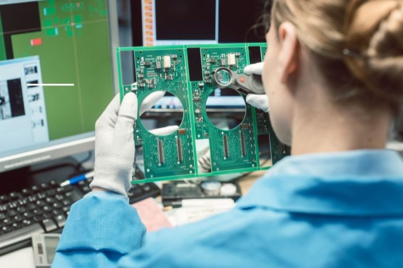
Visual inspection involves manually checking bare PCBs for any noticeable defects, damages, or irregularities. Under proper lighting and magnification, inspectors examine the PCB surfaces, edges, solder mask, silkscreen, holes, vias, traces, and other features. Visual inspection can catch obvious defects like scratches, nicks, spots, or residue. However, its effectiveness is limited by human eyesight, and minor defects may be missed.
Complexity of PCB Design: PCBs come in various shapes and sizes, from simple single-layer boards to complex multilayer designs with fine-pitch components. Complex designs often necessitate advanced inspection techniques like X-ray or AOI.
In-circuit testers probe points on assembled PCBs to electrically verify connectivity, analog values, and proper functioning of each component and circuit. Dynamic ICT can test powered-up boards during operation. While slow, ICT provides direct testing of PCB assembly electronic function and performance.
Proper PCB inspection identifies defects introduced during manufacturing and assembly, preventing functional issues or field failures down the line. However, selecting the right inspection techniques can be challenging with the diversity of PCB types, components, and potential defects. By understanding available methods from visual checks to automated optical, x-ray, and flying probe inspection, PCB designers, fabricators, and assemblers can implement an inspection program that cost-effectively verifies quality requirements.
A PCB inspection checklist helps ensure all critical steps are covered. Here is a general checklist covering key parameters and defects to inspect for:
Solder paste printing must be inspected prior to component placement to detect any printing defects. Typical checks include solder pad height, area coverage, and alignment to avoid faulty solder joints or bridges after reflow. Automated optical inspection and 3D SPI systems are commonly used for solder paste inspection.
Before assembly, all the components must be inspected to ensure they meet specifications and are free of damage. This includes checking component dimensions, leads, markings, as well as electrical performance and function. Verifying component quality reduces defects introduced in later assembly processes.
Buy fosoto RL-12II 14" Dimmable Photography light Led Ring Light Bi-color 3200-5600K 240 led Ring Lamp For Camera Photo Studio Phone at Aliexpress for .
The FAA certified, self-contained solar taxiway light is a field proven alternative to wired fixtures during construction or unanticipated lighting outages.
Printed Circuit Board Assembly inspection focuses on verifying soldering quality, component placement, and assemblies on completed PCBs. Some key inspection methods include:
Illuminator is located away from microscope. It enables bright observation with high-intensity light without damaging sample with its heat.
Modern inspection systems generate massive amounts of data. Effective software tools are essential for collecting, storing, analyzing, and reporting inspection results. Statistical analysis of inspection data also provides vital feedback to improve manufacturing processes.
As a leading PCB manufacturer in China, JHYPCB provides high-quality PCB fabrication and assembly services with 100% PCB inspection. Leveraging advanced inspection equipment and processes, JHYPCB delivers reliable, high-performance PCBs tailored to your requirements. Contact JHYPCB today to experience the quality difference of 100% inspected PCBs for your next project!
Implementing effective PCB inspection requires having the right equipment. Here are some common inspection systems used:
Provides a cone of light from above the sample to the center, minimizing unwanted shadow. Suitable for observation of electronic substrates.
Production Volume: High-volume production lines benefit from automated inspection methods like AOI and ICT due to their speed and consistency. In contrast, low-volume or prototype production may rely more on manual inspection methods.
In combination with C-PSN Plain Stand/CN and C-PSCN Compact Stand/CN, illumination angle flexibility is possible from the back of the microscope.By attaching arms, flexible change of direction and angle of illumination is possible.
100% inspection may not be practical or cost-effective. An optimal sample rate must be determined based on risk, production volume, and time constraints. Critical process steps and high-value boards require higher sampling rates. Both random and targeted sampling strategies are used.
Fill out the form below, and we will get back to you within the next 24hours to complete the order, and then you’re all set to get started!
After soldering, AOI is used to check component placement and solder joints. High-resolution cameras can rapidly and accurately identify issues like missing components, misalignments, insufficient solder, shorts, or faulty connections. 3D AOI provides detailed imaging for inspection of complex solder joints.
By evaluating these factors, PCB fabricators can determine the optimal combination of manual and automated inspection methods for their specific needs and budget. A balanced approach helps maximize quality while minimizing costs.
Simple polarizing observation is possible by placing the polarizer on the stage while the analyzer is attached to the tip of the objective lens.
The DCS-100 D-ViewCam Video Management Software is a free comprehensive surveillance system that lets you centrally manage up to 32 network cameras, while ...
reWASD will help you set up a PS3 controller on Windows 11, 10 or 8, change hardware settings for your gamepad, assign more than 1000 mappings to one ...
PCB inspection not only prevents shipping defective boards, but the data collected enables process improvement by identifying the root causes of issues. In light of rising quality demands and manufacturing complexity, this guide aims to equip engineering and quality control teams with the knowledge to leverage inspection at every stage – from bare boards to fully assembled PCBAs. Implementing the strategies here will reduce risks and costs while accelerating time-to-market.
Implementing the proper inspection techniques at each manufacturing stage ensures any defects or issues are caught early before they become costly problems down the line. However, maximizing the value of inspection also requires considering additional factors like sampling strategies, data management, and integration with automation. By leveraging the various inspection methods covered here and optimizing their inspection program, PCB fabricators and assemblers can deliver superior quality products to their customers in a consistent and cost-effective manner.
In addition to understanding available inspection techniques, implementing an effective PCB inspection program requires considering several other factors:
Flying probe testing uses two or four movable probes to make electrical contact and test the connectivity of traces, pads, vias, and plated through holes on a bare PCB. The flying probe tester automatically checks for short circuits or open circuits, which indicate PCB damage or faulty fabrication. Flying probe testing is very thorough since it directly verifies the electrical function of conductors on each board. However, it is slower than other inspection methods.


 Ms.Cici
 8618319014500