
Advanced Stereo Motor Sports, 11820 Magnolia Ave, ... - advanced stereo
As an alternative to CIDRE there is also BaSiC. There is an update site available for it and you can find a bit of demo/documentation here. If I remember correctly it does work on stacks and was quite fast.
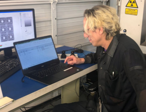
I was wondering whether there is an ImageJ workflow already for correcting brightfield illumination? I just tried an own attempt (median filter based) and I guess that would be OK but I also do not want to reinvent the wheel…
In fact, I do have more images. My naive approach was just to compute a median projection, thereby ideally removing the objects and only being left with the flat-field. This of course does not work very robustly if there are many objects in every image. Thus, thanks for pointing out CIDRE I will check it out!
Because PCBs have grown in complexity over the years, so too have inspections. As a result, professionals in the circuit board manufacturing industry can choose from a variety of inspection methods best suited to examine the board in question.
Inspection is a critical part of the PCB assembly process. Without it, electronics manufacturers would never know for sure whether the PCB—and therefore the device—would work properly. This could lead to a massive loss in sales, customers, and a big hit to reputation. Depending on the device, the result could even be harmful or deadly. To prevent such disastrous outcomes, PCB manufacturers incorporate various inspections throughout the design, fabrication, and assembly process.
Shop IKEA's LED light strips for endless creative lighting capabilities. Our modern LED strip lights are energy-efficient, fun and flexible.
Criticalillumination

One thing to keep in mind is that manufacturers don’t always use one single inspection technique. Many times, they use numerous inspections throughout the production process. In one stage, a technician may use the manual visual method, while in another they may utilize an X-ray lamination system.
PS: Here are again results obtained from the supplied sample image. Profiles are on the image diagonal from left bottom to right top.
In the case in question they zero out harmonic spatial waves of large periods. Division is the way to go but improved image acquisition is superior!
If you have many images from the same microscope under similar settings, you can estimate the flatfield with CIDRE https://github.com/smithk/cidre.
Integral images have been introduced in by Crow (1984)[1] as a technique to improve texture rendering speed at multiple scales in perspective projections. The technique has since then been used for a number of applications. The most popular...
Could you please test it? Update site: EMBL-CBA And then at the very bottom of Plugins > Restoration > Illumination > BaSiC (I am not sure it will work immediately because I had some strange dependency issues…)
This inspection method is similar to MVIs with the exception of using a PCB inspection machine rather than a human being to analyze the circuit board. The machine uses light to illuminate the board, followed by cameras that take pictures or videos of the PCB. Special software then compares the footage with design specifications or a preapproved finished product. AOIs are best used for more complicated or high-risk circuit boards, as they can better detect flaws, defects, and damage.
Manual visual inspections are ideal for simpler PCBs and clients who are on a tight budget. Automatic optical inspections, X-ray inspections, and laser tests are helpful for higher-risk PCBs, such as PCBs for medical, manufacturing, and automotive applications. X-ray inspections are also helpful for circuit boards featuring densely populated electrical components.
To better scrutinize complex circuit boards, manufacturers prefer to use X-ray technology. These inspections allow technicians to analyze smaller and more numerous components and chip packages, which often feature hidden solder connections. Technicians are also able to see bubbles in the solder work that wouldn’t otherwise be spotted. There are two types of X-ray inspections:
With so many different types of inspection methods available, technicians must match each PCB with the right technique. To do this, workers consider three factors:
to me it seems you need a flat-field correction. [https://en.wikipedia.org/wiki/Flat-field_correction] This means, you should divide by the correction, not subtract it (also the Fourier filters do a subtraction, not a division). Otherwise the features in the dark (insufficiently illuminated) parts of the image get too weak. You could try, e.g., the following macro:
Automatic Laser Test systems use lasers to inspect a PCB and take measurements. These measurements include height, solder joint dimensions, solder joint deposition, and reflectivity. The collected measurements are then compared to design specifications or a preapproved completed circuit board. Any inaccuracies, flaws, or defects will be uncovered during the comparison process.
I have now a similar dataset (a time-laps of 60 wells with 6x6 tiles per well in Brightfield) and it would be great if you would have code that I could use Thanks!
If you have more images than CDRE can digest or you’re interested in 3D flatfields (I gues you’re not ;)), you can use our not yet published scale up of the CIDRE approach https://github.com/saalfeldlab/stitching-spark.
Active Lighting and Its Application for Computer Vision: 40 Years of History of Active Lighting Techniques (Advances in Computer Vision and Pattern ...
Widefield microscope
Before we dive into our inside look into inspection methods and techniques in PCBA, or printed circuit board assembly, let’s talk a bit more about why PCB inspections are so important.
Great bright light with added strobing safety feature! Super simple installation, highly recommended! HitchMount LED Pod Reverse Kit. Item purchased ...
August,6 2021 An Inside Look: Inspection Methods and Techniques in PCBA Inspection is a critical part of the PCB assembly process. Without it, electronics manufacturers would never know for sure whether the PCB—and therefore the device—would work properly. This could lead to a massive loss in sales, customers, and a big hit to reputation. Depending on the device, the result could even be harmful or deadly. To prevent such disastrous outcomes, PCB manufacturers incorporate various inspections throughout the design, fabrication, and assembly process. Because PCBs have grown in complexity over the years, so too have inspections. As a result, professionals in the circuit board manufacturing industry can choose from a variety of inspection methods best suited to examine the board in question. Before we dive into our inside look into inspection methods and techniques in PCBA, or printed circuit board assembly, let’s talk a bit more about why PCB inspections are so important. The Importance of PCB Inspection As stated above, if a PCB isn’t inspected, its performance is a gamble. The component could perform well, or it could fail to function from the get-go. PCBs need to be inspected multiple times throughout the production process to: Catch defects early, whether it be a short circuit or improperly placed electrical component. Uncover design flaws that went unnoticed during the design stage. Once these defects or design flaws are discovered, technicians can take action to correct them, as well as note any potential mistakes to prevent them in the future. The Benefits of PCB Inspections In addition to a well-crafted circuit board, the benefits of PCB inspections are: Cost-savings. This benefit is threefold: By inspecting circuit boards throughout production, technicians can halt the process to catch flaws. As a result, manufacturers avoid wasting precious time and money fabricating a useless product. Customers will not demand warranty payments or institute returns for a quality PCB. A quality circuit board will likely not cause injury or death as a faulty PCB would, sparing the company from expensive litigation. Consistent quality. PCB inspections ensure that all circuit boards are created with the same level of quality, no matter their function or complexity. Improve manufacturing processes. If a defect or design flaw pops up again and again, it could be a sign that something needs to be adjusted in the production process. Once the culprit is uncovered, processes could be changed to prevent that flaw or defect from appearing in the future. Different PCB Inspection Techniques There are a variety of different inspection methods that take place in the printed circuit board assembly process. These techniques include: Manual visual inspections Automated optical inspections Automatic laser tests X-ray inspections Let’s take an inside look into the inspection methods and techniques in PCBA. Manual Visual Inspections Many times, PCB inspections use this method to start. During a manual visual inspection, a trained technician examines the circuit board with their eye or a magnifier. The technician will have a copy of the design documents with which to compare the board. This will help them determine whether all specifications are met and if there are any defects. They will also: Check for warpage Ensure that the board’s thickness and dimensions are correct Look for open circuits, burrs, solder bridging, pits, dents, pinholes, and scratches Inspect plating flux When compared with other inspection methods, MVIs are simple, affordable, and quick to complete. The only caveats are: Having a technician with the expertise needed to perform the inspections properly Inability to inspect what the technician cannot see (ex. Hidden solder joints, minuscule defects) Automated Optical Inspections This inspection method is similar to MVIs with the exception of using a PCB inspection machine rather than a human being to analyze the circuit board. The machine uses light to illuminate the board, followed by cameras that take pictures or videos of the PCB. Special software then compares the footage with design specifications or a preapproved finished product. AOIs are best used for more complicated or high-risk circuit boards, as they can better detect flaws, defects, and damage. Automatic Laser Tests Automatic Laser Test systems use lasers to inspect a PCB and take measurements. These measurements include height, solder joint dimensions, solder joint deposition, and reflectivity. The collected measurements are then compared to design specifications or a preapproved completed circuit board. Any inaccuracies, flaws, or defects will be uncovered during the comparison process. X-Ray Inspections To better scrutinize complex circuit boards, manufacturers prefer to use X-ray technology. These inspections allow technicians to analyze smaller and more numerous components and chip packages, which often feature hidden solder connections. Technicians are also able to see bubbles in the solder work that wouldn’t otherwise be spotted. There are two types of X-ray inspections: X-Ray Fluoroscopic System: This inspection method uses a beam of x-rays to analyze solder work and uncover defects such as cracks, bridging, and misalignment. X-Ray Lamination System: This method allows technicians to inspect different sections of PTH and BGA solder joints. How Is the Inspection Method Determined? With so many different types of inspection methods available, technicians must match each PCB with the right technique. To do this, workers consider three factors: Defects: The particular defect(s) that the manufacturer or client is most interested in uncovering. Cost: Some techniques are more affordable and more expensive than others. Speed: Some techniques are quicker to perform than others. In applications that require high production volumes, automated techniques are best. Manual visual inspections are ideal for simpler PCBs and clients who are on a tight budget. Automatic optical inspections, X-ray inspections, and laser tests are helpful for higher-risk PCBs, such as PCBs for medical, manufacturing, and automotive applications. X-ray inspections are also helpful for circuit boards featuring densely populated electrical components. Other aspects to consider when determining an inspection method are: Analyzing solder paste volume Uncovering solder defects Determining component positioning Discovering warpage Finding short circuits Checking polarity One thing to keep in mind is that manufacturers don’t always use one single inspection technique. Many times, they use numerous inspections throughout the production process. In one stage, a technician may use the manual visual method, while in another they may utilize an X-ray lamination system. Get a Quote
DCS Mechanical. Commercial & Residential Construction · Missouri, United States · <25 Employees. View Company Info for Free. About ...
There are a variety of different inspection methods that take place in the printed circuit board assembly process. These techniques include:
What magnification? If overall magnification is small, a normal Microscope may be sub-optimum and special illumination may be needed.
As an alternative to CIDRE there is also BaSiC . There is an update site available for it and you can find a bit of demo/documentation here . If I remember correctly it does work on stacks and was quite fast.
Just for the record (maybe other people will find this post interesting): CIDRE and BaSiC are giving very similar results for my data (just different treatment of the offset due to the particular CIDRE settings that I used): image2384×1478 1.06 MB
Your new code (right?): https://github.com/saalfeldlab/stitching-spark/blob/42e01a6fe2751980102922513df309ba25b00f70/src/main/java/org/janelia/stitching/experimental/IlluminationCorrectionSliceParallel.java#L1452
An LED lamp or LED light is an electric light that produces light using light-emitting diodes (LEDs). LED lamps are significantly more energy-efficient than ...
Once these defects or design flaws are discovered, technicians can take action to correct them, as well as note any potential mistakes to prevent them in the future.
CIDRE works really well! However I would need to write an other UI that enables batch-processing of many experiments and also accepts Tiff stacks as input. I guess it would make to use your new code as a starting point, rather than the original one?
unfortunately you didn’t use the provided sample image for your experiments. Furthermore, the provided sample image is JPG-compressed …
I have now a similar dataset (a time-laps of 60 wells with 6x6 tiles per well in Brightfield) and it would be great if you would have code that I could use Thanks!
Darkfieldmicroscopy
When you shop with us, you can find a bath light bar suitable for any bathroom large or small. We have bathroom lighting fixtures for every taste and style.
As stated above, if a PCB isn’t inspected, its performance is a gamble. The component could perform well, or it could fail to function from the get-go. PCBs need to be inspected multiple times throughout the production process to:
there are a few documented methods. From these, I found the FFT bandpass filter to work nice and fast, but the result using your image posted above is not necessarily of better quality compared to what you already have.
2019527 — Allied Vision is expanding its series of compact, rugged Mako G cameras with a new camera featuring polarization filter technology. The new Mako ...
Many times, PCB inspections use this method to start. During a manual visual inspection, a trained technician examines the circuit board with their eye or a magnifier. The technician will have a copy of the design documents with which to compare the board. This will help them determine whether all specifications are met and if there are any defects. They will also:

Our LED Linear Light Bars are an ultra-low profile, energy-efficient, and cost-effective lighting solution for Light Boxes & display lighting applications.
the BioVoxxel Pseudoflatfield correction with a radius around 10 also doesn´t look too bad and it´s super easy to use. There are some artifacts in the lower left corner which I guess are due to the jpeg format of the sample image.
Köhlerillumination
Artificially intelligent (AI) lighting controls offer a broad range of possibilities, impacting lighting design, installation, ...
Zebra VS40 Vision Camera Part #: VS40-SR20M4-2C00W | SKU: ZEB735243 ... Almost all production line inspection applications can be supported by the VS40's wide ...
If you’re only after a band pass, you could also try Plugins > Integral Image Filters > Normalize Local Contrast which is even faster than the FFT bandpass. Try various block-sizes with preview checked


 Ms.Cici
 8618319014500