
Image Studio Lite - image studio lite software
IndustrialPTZcamera

Special sensors are used in various applications such as creation of multi-spectral images, video laryngoscopes, gamma cameras, Flat-panel detectors and other sensor arrays for x-rays, microbolometer arrays in thermography, and other highly sensitive arrays for astronomy.[20]
USING ECS INCREASES YOUR OVERALL EQUIPMENT EFFECTIVENESS (OEE) BY TRACKING PROCESS CHARACTERISTICS FROM THE PRIMARY ASSET THROUGH VALUE ADD CONVERTING
While in general, digital cameras use a flat sensor, Sony prototyped a curved sensor in 2014 to reduce/eliminate Petzval field curvature that occurs with a flat sensor. Use of a curved sensor allows a shorter and smaller diameter of the lens with reduced elements and components with greater aperture and reduced light fall-off at the edge of the photo.[21]
Any of the solutions can be executed in the field from large permanent systems to small rolling or handheld configurations.
IndustrialCCTVcamera
Our LMPLN-IR and LCPLN-IR long working distance Plan Achromat lenses, are specifically designed for optimal transmission in the near infrared (700-1300nm ...
Visit us at the Automate event to learn how NVIDIA's AI platforms for manufacturing, robotics, and logistics are improving efficiency, scalability, ...
Cameras integrated in small consumer products generally use CMOS sensors, which are usually cheaper and have lower power consumption in battery powered devices than CCDs.[8] CCD sensors are used for high end broadcast quality video cameras, and CMOS sensors dominate in still photography and consumer goods where overall cost is a major concern. Both types of sensor accomplish the same task of capturing light and converting it into electrical signals.
The basis for modern solid-state image sensors is MOS technology,[23][24] which originates from the invention of the MOSFET by Mohamed M. Atalla and Dawon Kahng at Bell Labs in 1959.[25] Later research on MOS technology led to the development of solid-state semiconductor image sensors, including the charge-coupled device (CCD) and later the active-pixel sensor (CMOS sensor).[23][24]
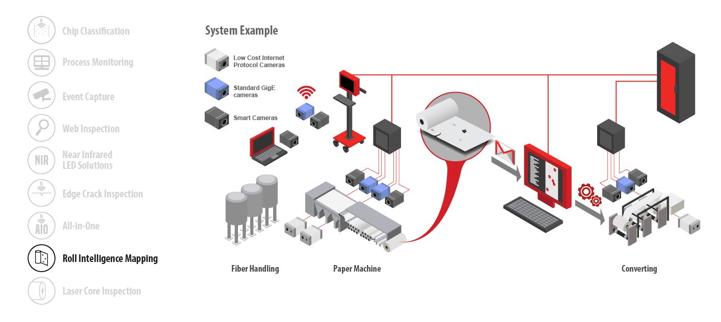
Web inspection data can be collected with additional process data on a per roll basis, and stored in the ECS process database
MOS image sensors are widely used in optical mouse technology. The first optical mouse, invented by Richard F. Lyon at Xerox in 1980, used a 5 μm NMOS integrated circuit sensor chip.[2][1] Since the first commercial optical mouse, the IntelliMouse introduced in 1999, most optical mouse devices use CMOS sensors.[36]
The NMOS active-pixel sensor (APS) was invented by Olympus in Japan during the mid-1980s. This was enabled by advances in MOS semiconductor device fabrication, with MOSFET scaling reaching smaller micron and then sub-micron levels.[6][32] The first NMOS APS was fabricated by Tsutomu Nakamura's team at Olympus in 1985.[33] The CMOS active-pixel sensor (CMOS sensor) was later improved by a group of scientists at the NASA Jet Propulsion Laboratory in 1993.[7] By 2007, sales of CMOS sensors had surpassed CCD sensors.[34] By the 2010s, CMOS sensors largely displaced CCD sensors in all new applications.
Machinecamera monitoring
Exposure time of image sensors is generally controlled by either a conventional mechanical shutter, as in film cameras, or by an electronic shutter. Electronic shuttering can be "global," in which case the entire image sensor area's accumulation of photoelectrons starts and stops simultaneously, or "rolling" in which case the exposure interval of each row immediate precedes that row's readout, in a process that "rolls" across the image frame (typically from top to bottom in landscape format). Global electronic shuttering is less common, as it requires "storage" circuits to hold charge from the end of the exposure interval until the readout process gets there, typically a few milliseconds later.[14]
1PC NEW Sony Industrial Camera XC-EI30CE Fast delivery ; Sp automation (38) ; Shipping, returns, and payments · International shipment of items may be subject to ...
Industrial camerasystem
We are a software company that designs, builds, installs and services camera based quality controls systems to increase process OEE (overall equipment effectiveness). Event Capture Systems, Inc. is the leading manufacturer of video event capture and inspection software solutions for the paper, packaging and related converting industries.
Our camera based quality control systems help increase the speed of the process while decreasing waste (defects and wasted material during process disruptions) and delay (downtime). Maintaining and increasing the realized capacity is not an option for today’s industries – it’s the key to survival and this task is not getting easier.
2019117 — MM stands for millimeters which describes the focal length of your lens. Lenses can either be of a fixed focal length also known as prime lens, ...
From a solution standpoint – ECS provides a wide selection of quality control solutions under three main groups that can be installed in two ways
In February 2018, researchers at Dartmouth College announced a new image sensing technology that the researchers call QIS, for Quanta Image Sensor. Instead of pixels, QIS chips have what the researchers call "jots." Each jot can detect a single particle of light, called a photon.[37]
2020831 — The Jesus myth is almost entirely lifted from Horus, the Egyptian God of the sun. Born of a virgin on Dec. 25, had 12 disciples, healed the blind, raised a man ...
Industrial processcameras
What We DoChip ClassificationProcess MonitoringEvent CaptureWeb InspectionWet Line Tracking with Twin IREdge Crack InspectionAll-in-OneRoll Intelligence Mapping
Find a great selection of Projector Lights at LightInTheBox. Get the Dresses, Tops,Sweaters and much more at a competitve price.
Early CCD sensors suffered from shutter lag. This was largely resolved with the invention of the pinned photodiode (PPD).[7] It was invented by Nobukazu Teranishi, Hiromitsu Shiraki and Yasuo Ishihara at NEC in 1980.[7][31] It was a photodetector structure with low lag, low noise, high quantum efficiency and low dark current.[7] In 1987, the PPD began to be incorporated into most CCD devices, becoming a fixture in consumer electronic video cameras and then digital still cameras. Since then, the PPD has been used in nearly all CCD sensors and then CMOS sensors.[7]
Early analog sensors for visible light were video camera tubes. They date back to the 1930s, and several types were developed up until the 1980s. By the early 1990s, they had been replaced by modern solid-state CCD image sensors.[22]
For example – a diaper starts from a rolled product 3 to 10 meters wide weighing several tons and is converted over multiple steps to create the highly engineered product used in a household. The overall realized capacity is a sum of the individual steps. RIM is the application of defect data from one process that is passed to the next process allowing these subsequent processes to optimize how it’s converted. A chain is only as strong as each individual link – RIM ensures each link in a multi-step process positively contributes to the overall realized capacity of the entire manufacturing cycle.
There are many parameters that can be used to evaluate the performance of an image sensor, including dynamic range, signal-to-noise ratio, and low-light sensitivity. For sensors of comparable types, the signal-to-noise ratio and dynamic range improve as the size increases. It is because in a given integration (exposure) time, more photons hit the pixel with larger area.
Wet line tracking. NIR lighting supports image processing programs that determine the positioning of wet lines along several parallel zones on the scene
Industrialcameras
OUR SOLUTION CAN IDENTIFY PROCESS DEFECTS IN HARSH CONDITIONS, AMBIENT LIGHT, OR MICRO WRINKLES WITH DEDICATED LED AND CAMERA BEAM CONFIGURATIONS
The first commercial digital camera, the Cromemco Cyclops in 1975, used a 32×32 MOS image sensor. It was a modified MOS dynamic RAM (DRAM) memory chip.[35]
THE ECS SMART CAMERA IS THE FOUNDATION OF THIS SOLUTION. EVERYTHING IS DONE BY THE CAMERA: IT ACQUIRES, PROCESSES, AND STORES THE INFORMATION ON BOARD
A CMOS image sensor has an amplifier for each pixel compared to the few amplifiers of a CCD. This results in less area for the capture of photons than a CCD, but this problem has been overcome by using microlenses in front of each photodiode, which focus light into the photodiode that would have otherwise hit the amplifier and not been detected.[9] Some CMOS imaging sensors also use Back-side illumination to increase the number of photons that hit the photodiode.[10] CMOS sensors can potentially be implemented with fewer components, use less power, and/or provide faster readout than CCD sensors.[11] They are also less vulnerable to static electricity discharges.
IndustrialCCTV solutions
Another design, a hybrid CCD/CMOS architecture (sold under the name "sCMOS") consists of CMOS readout integrated circuits (ROICs) that are bump bonded to a CCD imaging substrate – a technology that was developed for infrared staring arrays and has been adapted to silicon-based detector technology.[12] Another approach is to utilize the very fine dimensions available in modern CMOS technology to implement a CCD like structure entirely in CMOS technology: such structures can be achieved by separating individual poly-silicon gates by a very small gap; though still a product of research hybrid sensors can potentially harness the benefits of both CCD and CMOS imagers.[13]
5-Pin B Code M12 Straight Female Connector. $26.68. Item# M12.5B-SF-FM. Volume discounts available. Volume Discount Schedule.
In June 2022, Samsung Electronics announced that it had created a 200 million pixel image sensor. The 200MP ISOCELL HP3 has 0.56 micrometer pixels with Samsung reporting that previous sensors had 0.64 micrometer pixels, a 12% decrease since 2019. The new sensor contains 200 million pixels in a 1-by-1.4-inch (25 by 36 mm) lens.[28]
Micro-pulsed NIR. The short on-time of the NIR LED creates exceptional stop action clarity even with the camera operating at ‘open’ shutter’
The passive-pixel sensor (PPS) was the precursor to the active-pixel sensor (APS).[7] A PPS consists of passive pixels which are read out without amplification, with each pixel consisting of a photodiode and a MOSFET switch.[26] It is a type of photodiode array, with pixels containing a p-n junction, integrated capacitor, and MOSFETs as selection transistors. A photodiode array was proposed by G. Weckler in 1968.[6] This was the basis for the PPS.[7] These early photodiode arrays were complex and impractical, requiring selection transistors to be fabricated within each pixel, along with on-chip multiplexer circuits. The noise of photodiode arrays was also a limitation to performance, as the photodiode readout bus capacitance resulted in increased noise level. Correlated double sampling (CDS) could also not be used with a photodiode array without external memory.[6] However, in 1914 Deputy Consul General Carl R. Loop, reported to the state department in a Consular Report on Archibald M. Low's Televista system that "It is stated that the selenium in the transmitting screen may be replaced by any diamagnetic material".[27]
The charge-coupled device (CCD) was invented by Willard S. Boyle and George E. Smith at Bell Labs in 1969.[29] While researching MOS technology, they realized that an electric charge was the analogy of the magnetic bubble and that it could be stored on a tiny MOS capacitor. As it was fairly straightforward to fabricate a series of MOS capacitors in a row, they connected a suitable voltage to them so that the charge could be stepped along from one to the next.[23] The CCD is a semiconductor circuit that was later used in the first digital video cameras for television broadcasting.[30]
Save on Outdoor Spot Lights today, Why pay more? We offer Fast Delivery at the Lowest prices, shop safely with Australia's leading online Electrical ...
Clarity through the toughest steamy environments. NIR’s longer wavelength allows the light energy to penetrate the water vapor, hit the sheet and reflect back to the camera sensor.
A simple connection via Wi-Fi to the camera or by ethernet cable by any computer with a web browser is the complete solution
The two main types of digital image sensors are the charge-coupled device (CCD) and the active-pixel sensor (CMOS sensor), fabricated in complementary MOS (CMOS) or N-type MOS (NMOS or Live MOS) technologies. Both CCD and CMOS sensors are based on the MOS technology,[4] with MOS capacitors being the building blocks of a CCD,[5] and MOSFET amplifiers being the building blocks of a CMOS sensor.[6][7]
Make more visible to the camera. Because NIR is monochromatic it strips the color element out of the reflected light energy from the image.
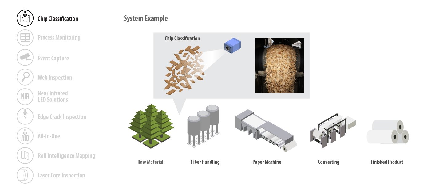
The mill can benchmark the actual chip quality parameter against set quality standards to determine corrective actions to provide optimum outcome of this raw material as it becomes paper
DETERMINE THE 2-DIMENSIONAL PROFILE OF THE CORE AND SURROUNDING ROLL BUILD TO DETERMINE IF THERE ARE PROTRUSIONS OR BASINS WITH 99.9% ACCURACY
Because these solutions become such a long-term and integral and critical aspect of best practices for our installed base – ECS understands we must become a partner in all aspects of the product lifecycle of these camera based solutions. We must be focused at all times on not only on how our systems are developed and built – but equally as important is the quality of installation and support. Our systems cannot afford to fail the operator and management when it’s needed most. In other words – we help increase uptime of your process – so the uptime of the camera based quality control system should never the problem.
Degree Chart for Bachelor of Science in Engineering (Course 2-A)
Each cell of a CCD image sensor is an analog device. When light strikes the chip it is held as a small electrical charge in each photo sensor. The charges in the line of pixels nearest to the (one or more) output amplifiers are amplified and output, then each line of pixels shifts its charges one line closer to the amplifiers, filling the empty line closest to the amplifiers. This process is then repeated until all the lines of pixels have had their charge amplified and output.[9]
Production linemonitoring camera
An image sensor or imager is a sensor that detects and conveys information used to form an image. It does so by converting the variable attenuation of light waves (as they pass through or reflect off objects) into signals, small bursts of current that convey the information. The waves can be light or other electromagnetic radiation. Image sensors are used in electronic imaging devices of both analog and digital types, which include digital cameras, camera modules, camera phones, optical mouse devices,[1][2][3] medical imaging equipment, night vision equipment such as thermal imaging devices, radar, sonar, and others. As technology changes, electronic and digital imaging tends to replace chemical and analog imaging.
The two main types of electronic image sensors are the charge-coupled device (CCD) and the active-pixel sensor (CMOS sensor). Both CCD and CMOS sensors are based on metal–oxide–semiconductor (MOS) technology, with CCDs based on MOS capacitors and CMOS sensors based on MOSFET (MOS field-effect transistor) amplifiers. Analog sensors for invisible radiation tend to involve vacuum tubes of various kinds, while digital sensors include flat-panel detectors.
Proactive Remote Monitoring (PRM)SmartFlex™IR LightingRepetitive Motion Analysis (RMA)Virtual Machine (VM)Directional Analysis
Flash blindness occurs when an extremely bright flash is discharged, usually at night, and again vision is temporarily lost." The United States Federal ...
An online and real-time camera-based inspection system positioned to monitor the wood chips from an incoming source can provide a breakdown of key wood chip parameters per time unit
See more without distractions. Reflected NIR energy from metal surfaces is less blinding to the camera sensor than reflected white light.
Able to be installed with a wide range of different mill configurations (working distance, field of view, space for equipment)


 Ms.Cici
 8618319014500