
Vapor Barriers or Vapor Retarders - define retarder
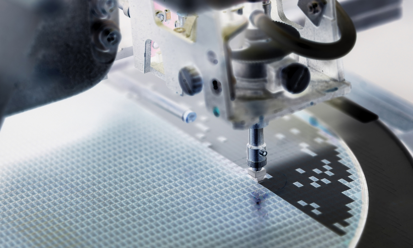
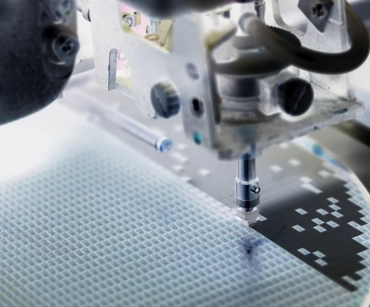
Figure 6 summarizes how an InP photonic device looks after the steps of layer epitaxy, etching, dielectric deposition and planarization, and metallization.
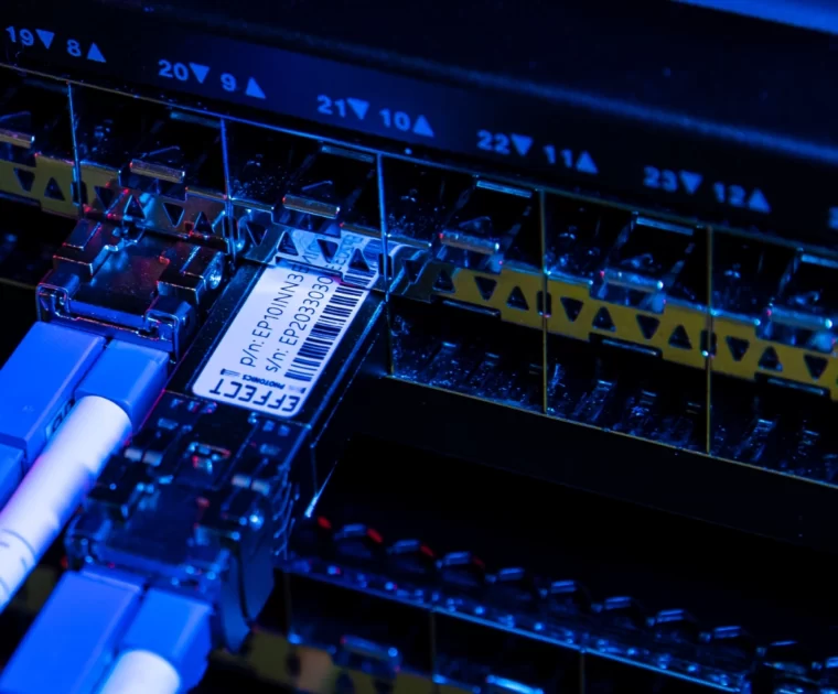
While packaging, assembly, and testing are only a small part of the cost of electronic systems, the reverse happens with photonic systems. Researchers at the Technical University of Eindhoven (TU/e) estimate that for most Indium Phosphide (InP) photonics devices, the cost of packaging, assembly, and testing can reach around 80% of the total module cost. There are many research efforts in motion to reduce these costs, which you can learn more about in one of our previous articles.
120mmto inches fraction
Aug 7, 2020 — 1812, "state of having different properties on different sides," from polarize + -ation, and in part from French polarisation, noun of action ...
Real life is, of course, a lot more complicated and will require cycling through these steps tens of times, leading to processes with more than 200 total steps. Let’s go through these basic steps in a bit more detail.
120 mm to feet
It is fresnel screen,Ultra bright. Note: place the fresnel in front of the ground glass, the matt surface towards the lens, the bright surface towards the ...
Given its importance, we want to explain how photonic integrated circuits (PICs), the devices that enable all these applications, are made.
120mm is what sizein inches
The AR Coating of an optical system is a dielectric thin layer typically applied to transmissive optics in order to reduce the reflectance of the light ...
120mmto inches to feet
2013429 — Understanding Microscope Objectives · Achromatic objectives–This objective brings red and blue light to a common focus, and is corrected for ...
Chip fabrication is a process with many sources of variability, and therefore much testing is required to make sure that the fabricated chip agrees with what was originally designed and simulated. Once that is certified and qualified, the process of packaging and assembling a device with the PIC follows.
1200 mm to inches
Jun 8, 2020 — 1 Answer 1 ... As a first observation, there is no maximum order. There is however a maximum propagating order, for which sinθs=1. Higher orders ...
The process of designing a PIC should translate an initial application concept into a functioning photonics chip that can be manufactured. In a short course at the OFC 2018 conference, Wim Bogaerts from Ghent University summarized the typical PIC design process in the steps we will describe below.
by C Yang · 2020 · Cited by 9 — Physical Chemistry Chemical Physics. Polarization-dependent vibrational shifts on dielectric substrates†. Check for updates. C. Yang,ab W. Wang,b A. Nefedov ...
Photonics is one of the enabling technologies of the future. Light is the fastest information carrier in the universe and can transmit this information while dissipating less heat and energy than electrical signals. Thus, photonics can dramatically increase the speed, reach, and flexibility of communication networks and cope with the ever-growing demand for more data. And it will do so at a lower energy cost, decreasing the Internet’s carbon footprint. Meanwhile, fast and efficient photonic signals have massive potential for sensing and imaging applications in medical devices, automotive LIDAR, agricultural and food diagnostics, and more.
The process of making photonic integrated circuits is incredibly long and complex, and the steps we described in this article are a mere simplification of the entire process. It requires tremendous amount of knowledge in chip design, fabrication, and testing from experts in different fields all around the world. EFFECT Photonics was founded by people who fabricated these chips themselves, understand the process intimately, and developed the connections and network to develop cutting-edge PICs at scale.
120mm is what sizein cm
Manufacturing semiconductor chips for photonics and electronics is one of the most complex procedures in the world. For example, back in his university days, EFFECT Photonics President Boudewijn Docter described a fabrication process with a total of 243 steps!
120 millimeters to inches
120mmto cm
© 2024 EFFECT PHOTONICS All rights reserved. T&C of Website - T&C of Purchase - Privacy Policy - Cookie Policy - Supplier Code of Conduct
Sep 3, 2021 — The focal length of your film or digital camera lens dictates how much of the scene your camera will be able to capture. Smaller numbers have a ...
Nov 11, 2021 — AI-generated answer. When a sound source moves towards a stationary observer, the wavelength of the sound is affected in the following way: (a) ...
The phenomenon in which electromagnetic waves, such as light waves, vibrate in a preferred plane or planes; or the process of confining the vibrations to ...
To magnify the image to the next level rotate the nosepiece to the 10X objective. While looking through the eyepiece focus the image into view using only the ...
Yuqing Jiao, Associate Professor at the Eindhoven University of Technology (TU/e), explains the fabrication process in a few basic, simplified steps:
Especially after the first fabrication run of a new chip, there will be a few rounds of characterization, validation and revisions to make sure the chip performs up to spec. After this first round of characterization and validation, the chip must be made ready for mass production, which requires a series of reliability tests in several environmental different conditions. You can learn more about this process in our previous article on industrial hardening. For example, different applications need different certification of the temperatures in which the chip must operate in.


 Ms.Cici
 8618319014500