
The History of Refracting Telescope - refracting telescope parts
General Manager at Edmend Construction · Experience: Edmend Construction · Education: Adama Science and Technology University (ASTU) · Location: Ethiopia ...
Flat lenssunglasses
T Suzuki · 2015 · 117 — We propose and experimentally demonstrate a new method called SF-STAMP for sequentially timed all-optical mapping photography (STAMP) that utilizes spectral ...
Flat lenscamera
Conventional cameras and imaging systems are not sensitive to light’s polarization state. In order to measure this fundamental degree-of-freedom of light, imaging systems must often rely on complex beam paths, moving parts, or special sensors. Using a metasurface, however, all polarization components necessary for a full measurement of light’s polarization state can be combined into a single optical element, rendering a polarization-measuring camera not altogether more complicated than an ordinary one; this has broad potential applications in remote sensing and machine vision.For more information, see Harvard SEAS news.
by JT HOLLADAY — Spherical aberration is the property of a single spheri- cal surface to refract rays too strongly as one moves from the center of the pupil peripherally ...
AR coatings for IR substrates have been tested to meet Military Specifications for adhesion, abrasion, temperature and humidity. These coatings may be cleaned ...
Opticalflatmeasurement
OpticalFlatMitutoyo
Jul 14, 2022 — The problem you face is a LASER diode emits a very narrow beam and detecting devices have a very narrow area of focus. Unlike a for example a TV ...
Can't find the option for it in settings. https://i.imgur.com/RZ1JSeN.png This one.
Create an account now for exclusive benefits, personalized recommendations, and seamless order tracking. Elevate your lab experience today!
Airy disc definition: the bright central part of the diffraction pattern of light from a point source that is diffracted by a circular aperture.
An independent marketplace for buying and selling new, used and refurbished lab equipment and supplies. A leader in the industry since 1995.
Flat lens opticsreview
Above: a near-infrared metalens employed in Coherent Raman scattering imaging (APL Photonics 6, 096107, 2021). Render by Kerolos M.A. Yousef.
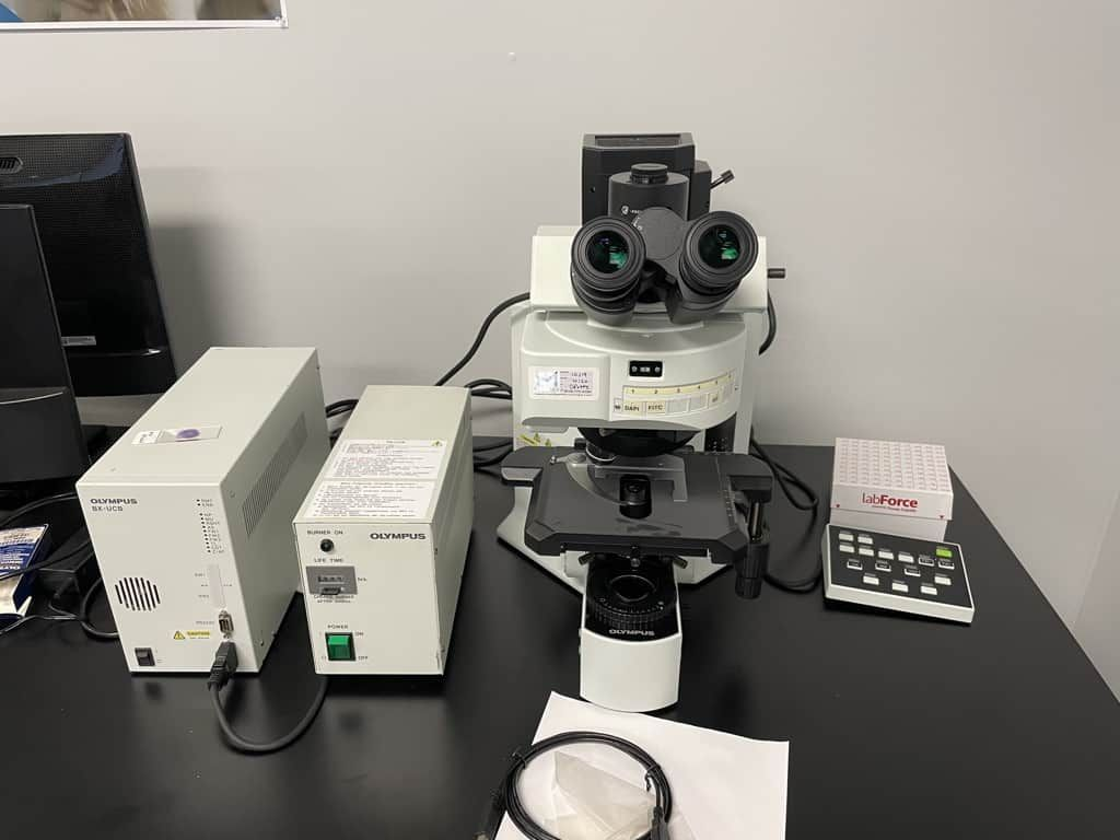
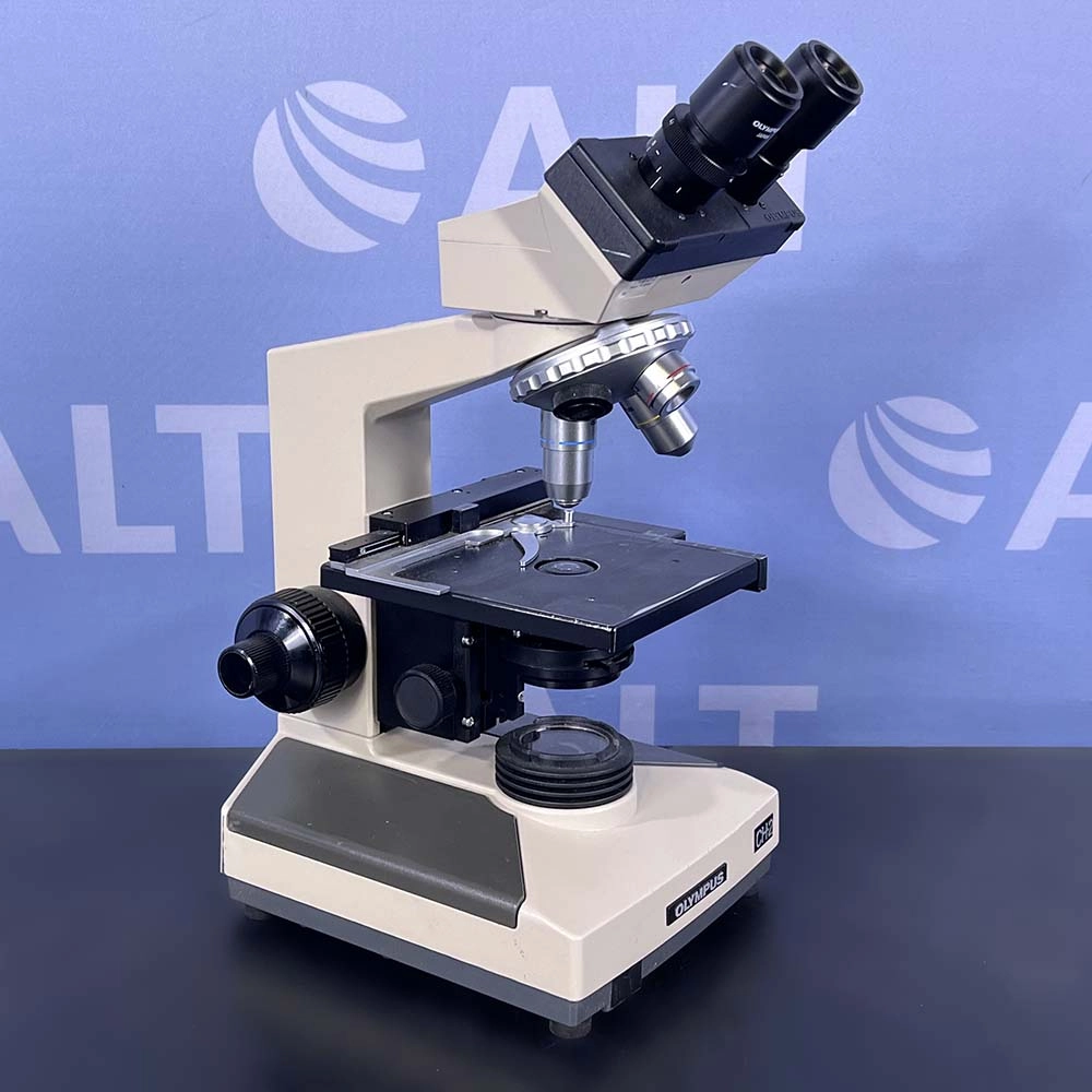
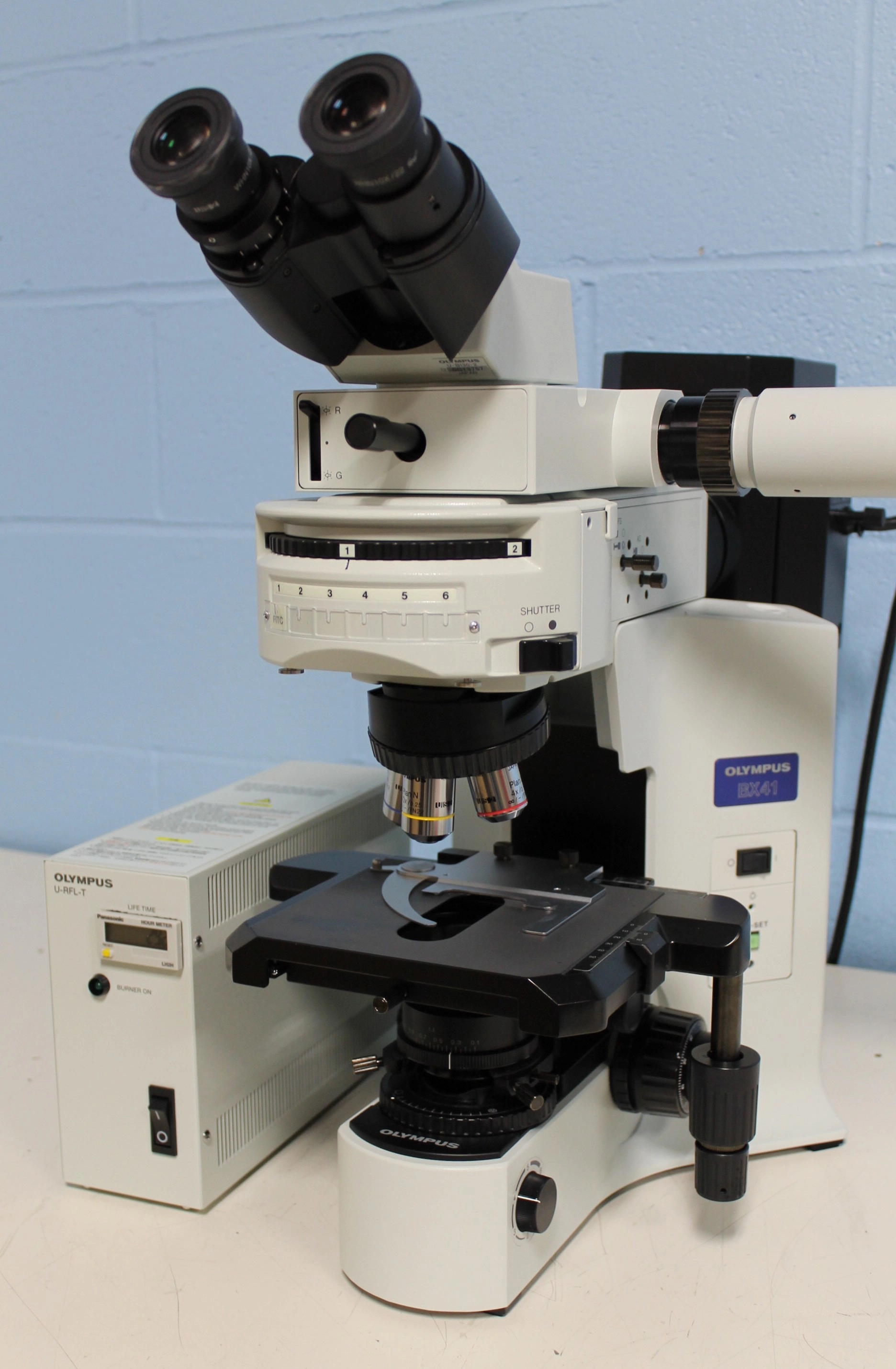
Online auctions and classified ads are available for buying and selling Olympus Microscopes. Find new and used Olympus Microscopes listings below. Contact sellers for a price or run a free wanted ad to locate the microscope or microscope parts you need.
In lens design, the most widely used approach for chromatic aberration correction is based on adding refractive lenses made of different glasses. This approach not only increases volume and weight, but also relies on the difficult process of developing new glasses with suitable dispersion properties. Here, we demonstrated a metasurface aberration corrector (metacorrector) whose phase and dispersion (group delay and group delay dispersion) profiles are tailored to correct the monochromatic and chromatic aberrations of a fused silica singlet. The metacorrector was designed by engineering the effective refractive index of each constituent nanostructure over a large bandwidth. The images above show experimental imaging results under incoherent white-light illumination for cases with and without the metacorrector. The same design method is applicable for sophisticated microscope objectives and is promising for realizing super-achromatic and diffraction-limited lenses.
Flat lensGlasses
Flat lensexamples
SKU, 582-4010. Name, Mounted Silicon Photodiode, (350-1100 nm), Anode Grounded. Spectral Region, 89,88. Active Area (diameter or square), 10+mm.
Metalenses are flat lenses that are ultrathin and lightweight, and are typically realized by placing millions to billions of nano-structures on a surface. The large number of structures makes scalability in both size and production scale a major concern. In our recent work, we demonstrate mass-producible, all-glass, centimeter-scale metalenses capable of focusing visible light, using deep-ultraviolet (DUV) projection lithography, a manufacturing technique widely used by computer chip foundries. These metalenses exhibit diffraction-limited performance and are suitable for potential applications in virtual reality (VR) devices and biological imaging techniques. Since the metalenses are also very light, we believe that they are ideal for camera applications where payload weight and footprint size are important, such as in drones and cubesats.
Flat lensvs curvedlens
Traditional optics - lenses, waveplates, filters, and the like - have existed for centuries. In many cases these elements are fashioned by techniques like machining and turning glass that, despite refinements, have also gone largely unchanged. More recently, metasurface optics have emerged where phase-shifting occurs at wavelength-scale, offering compactness and new functionality not accessible with bulk optical elements. These metasurface devices are fabricated using lithography, thin film deposition, and etching, techniques borrowed from semiconductor manufacturing. The production of these devices can be scaled up, with major consequences for optics.
This can mean that several components may be required to get the desired result. The non-spherical surface of an aspheric lens allows a ...
Termine per E‐Mail und Telefon vereinbaren. Besuche bei der Ausländerbehörde in der Eberhardstraße 39 sind nur noch mit Terminbestätigung möglich. Die ...
One of the applications of flat lenses is in spectroscopy. Optical spectroscopy is an essential tool used in many areas such as food monitoring and medical diagnostics. However, spectrometers typically face a trade-off between their spectral resolution, working wavelength range and overall device size due to optical aberrations in their focusing elements. To preserve high spectral resolution over a broad bandwidth, additional corrective optical components must be used. These add significant bulk and prevent easy integration with portable devices. Here we present a highly compact, aberration-corrected spectrometer using meta-lenses, which are comprised of subwavelength scale nanostructures. It achieves nanometer resolution across 200 nm in the visible spectrum, with an overall footprint at the centimeter-scale.
Metasurfaces comprise sub-wavelength nanostructures. By the design and arrangement of the constituent nanostructures, metasurfaces are able to impart customized polarization, amplitude and phase to incident light. Additionally, metasurfaces can be lithographically mass-produced, enabling miniature and multifunctional metasurface optical elements. Metalenses, as an example of metasurface optical elements, has attracted widespread attention and was hailed as one of the top ten emerging technologies of 2019 by the World Economic Forum and Scientific American. The group is working on developing large diameter, high-efficiency and achromatic metalenses for applications in imaging, illumination, virtual and augmented reality etc. Here are three YouTube videos for those who are interested to learn more:


 Ms.Cici
 8618319014500