
Prism Sights - Optics & Mounts - prism optics
Sarfus is a recent optical technique that increases the sensitivity of a standard optical microscope to a point where it is possible to directly visualize nanometric films (down to 0.3 nanometre) and isolated nano-objects (down to 2 nm-diameter). The technique is based on the use of non-reflecting substrates for cross-polarized reflected light microscopy.
In fluorescence microscopy many wavelengths of light ranging from the ultraviolet to the visible can be used to cause samples to fluoresce, which allows viewing by eye or with specifically sensitive cameras.
Scanning probe microscopes also analyze a single point in the sample and then scan the probe over a rectangular sample region to build up an image. As these microscopes do not use electromagnetic or electron radiation for imaging they are not subject to the same resolution limit as the optical and electron microscopes described above.
The performance of a compound light microscope depends on the quality and correct use of the condensor lens system to focus light on the specimen and the objective lens to capture the light from the specimen and form an image.[5] Early instruments were limited until this principle was fully appreciated and developed from the late 19th to very early 20th century, and until electric lamps were available as light sources. In 1893 August Köhler developed a key principle of sample illumination, Köhler illumination, which is central to achieving the theoretical limits of resolution for the light microscope. This method of sample illumination produces even lighting and overcomes the limited contrast and resolution imposed by early techniques of sample illumination. Further developments in sample illumination came from the discovery of phase contrast by Frits Zernike in 1953, and differential interference contrast illumination by Georges Nomarski in 1955; both of which allow imaging of unstained, transparent samples.
A microscope (from Ancient Greek μικρός (mikrós) 'small' and σκοπέω (skopéō) 'to look (at); examine, inspect') is a laboratory instrument used to examine objects that are too small to be seen by the naked eye. Microscopy is the science of investigating small objects and structures using a microscope. Microscopic means being invisible to the eye unless aided by a microscope.
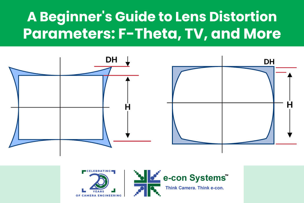
Basically, the cropping resolution is determined by dividing the source resolution by the zoom factor, and then this cropped region is resized to the final output resolution. This resizing is important for maintaining the frame size, but it invariably leads to a decrease in image quality.
In the early 20th century a significant alternative to the light microscope was developed, an instrument that uses a beam of electrons rather than light to generate an image. The German physicist, Ernst Ruska, working with electrical engineer Max Knoll, developed the first prototype electron microscope in 1931, a transmission electron microscope (TEM). The transmission electron microscope works on similar principles to an optical microscope but uses electrons in the place of light and electromagnets in the place of glass lenses. Use of electrons, instead of light, allows for much higher resolution.
ZoomOptics Binoculars
Scanning acoustic microscopes use sound waves to measure variations in acoustic impedance. Similar to Sonar in principle, they are used for such jobs as detecting defects in the subsurfaces of materials including those found in integrated circuits. On February 4, 2013, Australian engineers built a "quantum microscope" which provides unparalleled precision.[30]
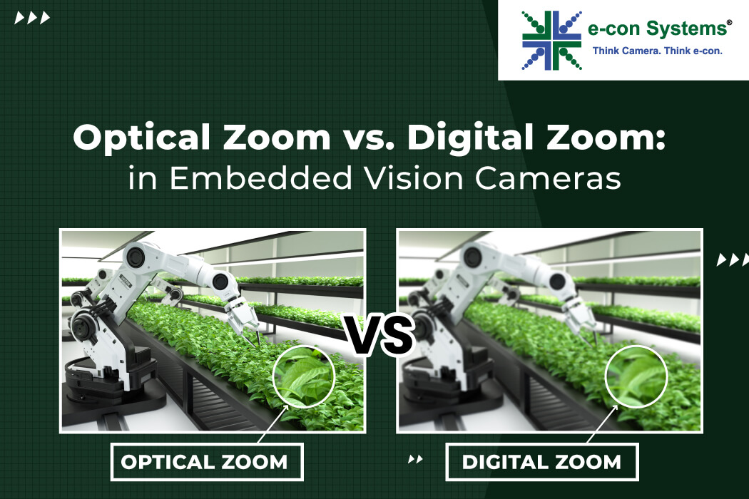
Optical zoom and digital zoom represent two different approaches to magnification in camera technology. Optical zoom, relying on the physical adjustment of lens elements, offers a tangible alteration in the image’s focal length, preserving image quality at various magnifications. In contrast, digital zoom, which employs software algorithms to crop and enlarge the image, presents a more flexible yet resolution-dependent method.
The most recent developments in light microscope largely centre on the rise of fluorescence microscopy in biology.[21] During the last decades of the 20th century, particularly in the post-genomic era, many techniques for fluorescent staining of cellular structures were developed.[21] The main groups of techniques involve targeted chemical staining of particular cell structures, for example, the chemical compound DAPI to label DNA, use of antibodies conjugated to fluorescent reporters, see immunofluorescence, and fluorescent proteins, such as green fluorescent protein.[22] These techniques use these different fluorophores for analysis of cell structure at a molecular level in both live and fixed samples.
There are many types of microscopes, and they may be grouped in different ways. One way is to describe the method an instrument uses to interact with a sample and produce images, either by sending a beam of light or electrons through a sample in its optical path, by detecting photon emissions from a sample, or by scanning across and a short distance from the surface of a sample using a probe. The most common microscope (and the first to be invented) is the optical microscope, which uses lenses to refract visible light that passed through a thinly sectioned sample to produce an observable image. Other major types of microscopes are the fluorescence microscope, electron microscope (both the transmission electron microscope and the scanning electron microscope) and various types of scanning probe microscopes.[1]
These zoom technologies, each with distinct advantages and limitations, play a crucial role in the functionality and application of modern camera systems across various sectors. So, let’s start exploring these topics in detail.
ZoomOptics as seen on TV
Much current research (in the early 21st century) on optical microscope techniques is focused on development of superresolution analysis of fluorescently labelled samples. Structured illumination can improve resolution by around two to four times and techniques like stimulated emission depletion (STED) microscopy are approaching the resolution of electron microscopes.[23] This occurs because the diffraction limit is occurred from light or excitation, which makes the resolution must be doubled to become super saturated. Stefan Hell was awarded the 2014 Nobel Prize in Chemistry for the development of the STED technique, along with Eric Betzig and William Moerner who adapted fluorescence microscopy for single-molecule visualization.[24]
Zoom opticreddit
Although objects resembling lenses date back 4,000 years and there are Greek accounts of the optical properties of water-filled spheres (5th century BC) followed by many centuries of writings on optics, the earliest known use of simple microscopes (magnifying glasses) dates back to the widespread use of lenses in eyeglasses in the 13th century.[2][3][4] The earliest known examples of compound microscopes, which combine an objective lens near the specimen with an eyepiece to view a real image, appeared in Europe around 1620.[5] The inventor is unknown, even though many claims have been made over the years. Several revolve around the spectacle-making centers in the Netherlands, including claims it was invented in 1590 by Zacharias Janssen (claim made by his son) or Zacharias' father, Hans Martens, or both,[6][7] claims it was invented by their neighbor and rival spectacle maker, Hans Lippershey (who applied for the first telescope patent in 1608),[8] and claims it was invented by expatriate Cornelis Drebbel, who was noted to have a version in London in 1619.[9][10] Galileo Galilei (also sometimes cited as compound microscope inventor) seems to have found after 1610 that he could close focus his telescope to view small objects and, after seeing a compound microscope built by Drebbel exhibited in Rome in 1624, built his own improved version.[11][12][13] Giovanni Faber coined the name microscope for the compound microscope Galileo submitted to the Accademia dei Lincei in 1625[14] (Galileo had called it the occhiolino 'little eye'). René Descartes (Dioptrique, 1637) describes microscopes wherein a concave mirror, with its concavity towards the object, is used, in conjunction with a lens, for illuminating the object, which is mounted on a point fixing it at the focus of the mirror.[15]
Despite significant advancements in digital imaging technologies, optical zoom maintains its significance in many embedded camera applications. One of the primary reasons is its ability to preserve image quality at various levels of magnification.
BuyZoomOptics
The two major types of electron microscopes are transmission electron microscopes (TEMs) and scanning electron microscopes (SEMs).[21][22] They both have series of electromagnetic and electrostatic lenses to focus a high energy beam of electrons on a sample. In a TEM the electrons pass through the sample, analogous to basic optical microscopy.[21] This requires careful sample preparation, since electrons are scattered strongly by most materials.[22] The samples must also be very thin (below 100 nm) in order for the electrons to pass through it.[21][22] Cross-sections of cells stained with osmium and heavy metals reveal clear organelle membranes and proteins such as ribosomes.[22] With a 0.1 nm level of resolution, detailed views of viruses (20 – 300 nm) and a strand of DNA (2 nm in width) can be obtained.[22] In contrast, the SEM has raster coils to scan the surface of bulk objects with a fine electron beam. Therefore, the specimen do not necessarily need to be sectioned, but coating with a nanometric metal or carbon layer may be needed for nonconductive samples.[21] SEM allows fast surface imaging of samples, possibly in thin water vapor to prevent drying.[21][22]
New types of scanning probe microscope have continued to be developed as the ability to machine ultra-fine probes and tips has advanced.
The rise of fluorescence microscopy drove the development of a major modern microscope design, the confocal microscope. The principle was patented in 1957 by Marvin Minsky, although laser technology limited practical application of the technique. It was not until 1978 when Thomas and Christoph Cremer developed the first practical confocal laser scanning microscope and the technique rapidly gained popularity through the 1980s.
The different types of scanning probe microscopes arise from the many different types of interactions that occur when a small probe is scanned over and interacts with a specimen. These interactions or modes can be recorded or mapped as function of location on the surface to form a characterization map. The three most common types of scanning probe microscopes are atomic force microscopes (AFM), near-field scanning optical microscopes (NSOM or SNOM, scanning near-field optical microscopy), and scanning tunneling microscopes (STM).[28] An atomic force microscope has a fine probe, usually of silicon or silicon nitride, attached to a cantilever; the probe is scanned over the surface of the sample, and the forces that cause an interaction between the probe and the surface of the sample are measured and mapped. A near-field scanning optical microscope is similar to an AFM but its probe consists of a light source in an optical fiber covered with a tip that has usually an aperture for the light to pass through. The microscope can capture either transmitted or reflected light to measure very localized optical properties of the surface, commonly of a biological specimen. Scanning tunneling microscopes have a metal tip with a single apical atom; the tip is attached to a tube through which a current flows.[29] The tip is scanned over the surface of a conductive sample until a tunneling current flows; the current is kept constant by computer movement of the tip and an image is formed by the recorded movements of the tip.[28]
If you require any help integrating a world-class camera into your product, please write to camerasolutions@e-consystems.com.
Let’s compare two cameras—one equipped with a 2MP resolution featuring optical zoom and the other a 20MP resolution with digital zoom capabilities.
Wide field optical microscopes and transmission electron microscopes both use the theory of lenses (optics for light microscopes and electromagnet lenses for electron microscopes) in order to magnify the image generated by the passage of a wave transmitted through the sample, or reflected by the sample. The waves used are electromagnetic (in optical microscopes) or electron beams (in electron microscopes). Resolution in these microscopes is limited by the wavelength of the radiation used to image the sample, where shorter wavelengths allow for a higher resolution.[21]
Ultraviolet light enables the resolution of microscopic features as well as the imaging of samples that are transparent to the eye. Near infrared light can be used to visualize circuitry embedded in bonded silicon devices, since silicon is transparent in this region of wavelengths.
Firstly, the 20MP camera captures far more detail initially, providing a richer source image from which to crop and zoom. Digital zoom also involves software algorithms that can apply sharpening and noise reduction to the cropped image, potentially enhancing clarity. Finally, there is more flexibility in post-production to refine the image, adjust the crop, apply corrections, etc.
X-ray microscopes are instruments that use electromagnetic radiation usually in the soft X-ray band to image objects. Technological advances in X-ray lens optics in the early 1970s made the instrument a viable imaging choice.[25] They are often used in tomography (see micro-computed tomography) to produce three dimensional images of objects, including biological materials that have not been chemically fixed. Currently research is being done to improve optics for hard X-rays which have greater penetrating power.[25]
One of the latest discoveries made about using an electron microscope is the ability to identify a virus.[19] Since this microscope produces a visible, clear image of small organelles, in an electron microscope there is no need for reagents to see the virus or harmful cells, resulting in a more efficient way to detect pathogens.
Digital microscopy with very low light levels to avoid damage to vulnerable biological samples is available using sensitive photon-counting digital cameras. It has been demonstrated that a light source providing pairs of entangled photons may minimize the risk of damage to the most light-sensitive samples. In this application of ghost imaging to photon-sparse microscopy, the sample is illuminated with infrared photons, each of which is spatially correlated with an entangled partner in the visible band for efficient imaging by a photon-counting camera.[27]
Scanning optical and electron microscopes, like the confocal microscope and scanning electron microscope, use lenses to focus a spot of light or electrons onto the sample then analyze the signals generated by the beam interacting with the sample. The point is then scanned over the sample to analyze a rectangular region. Magnification of the image is achieved by displaying the data from scanning a physically small sample area on a relatively large screen. These microscopes have the same resolution limit as wide field optical, probe, and electron microscopes.
Microscopes can be separated into several different classes. One grouping is based on what interacts with the sample to generate the image, i.e., light or photons (optical microscopes), electrons (electron microscopes) or a probe (scanning probe microscopes). Alternatively, microscopes can be classified based on whether they analyze the sample via a scanning point (confocal optical microscopes, scanning electron microscopes and scanning probe microscopes) or analyze the sample all at once (wide field optical microscopes and transmission electron microscopes).
The traditional optical microscope has more recently evolved into the digital microscope. In addition to, or instead of, directly viewing the object through the eyepieces, a type of sensor similar to those used in a digital camera is used to obtain an image, which is then displayed on a computer monitor. These sensors may use CMOS or charge-coupled device (CCD) technology, depending on the application.
Optical zoom, unlike digital zoom, involves the physical adjustment of lens elements, changing the focal length without altering the original pixel count of the image. It means the image retains its original resolution and clarity, even when zoomed in. Other reasons include better performance in low light conditions compared to digital zoom and more suitable for applications requiring zooming from a distance.
Transmission electron microscopes became popular following the Second World War. Ernst Ruska, working at Siemens, developed the first commercial transmission electron microscope and, in the 1950s, major scientific conferences on electron microscopy started being held. In 1965, the first commercial scanning electron microscope was developed by Professor Sir Charles Oatley and his postgraduate student Gary Stewart, and marketed by the Cambridge Instrument Company as the "Stereoscan".
Zoomoptics Amazon
Optical zoom in embedded cameras is characterized by the physical alteration of the camera lens’s focal length. This is achieved through the movement of glass elements within the lens assembly. By changing the distance between these elements, it becomes possible for the camera to easily zoom in or out on a subject. This mechanical adjustment allows for a variable field of view while maintaining the integrity of the image sensor’s resolution.
Digital zoom employs a software-centric approach rather than mechanical lens adjustments. Leveraging the Image Signal Processor (ISP) or camera software, digital zooming involves selecting and cropping a specific region from the camera’s source frame and then resizing this cropped area to match the desired resolution. This process is completely managed by the camera’s computational capabilities and doesn’t involve any physical alteration of the camera’s optics.
From 1981 to 1983 Gerd Binnig and Heinrich Rohrer worked at IBM in Zürich, Switzerland to study the quantum tunnelling phenomenon. They created a practical instrument, a scanning probe microscope from quantum tunnelling theory, that read very small forces exchanged between a probe and the surface of a sample. The probe approaches the surface so closely that electrons can flow continuously between probe and sample, making a current from surface to probe. The microscope was not initially well received due to the complex nature of the underlying theoretical explanations. In 1984 Jerry Tersoff and D.R. Hamann, while at AT&T's Bell Laboratories in Murray Hill, New Jersey began publishing articles that tied theory to the experimental results obtained by the instrument. This was closely followed in 1985 with functioning commercial instruments, and in 1986 with Gerd Binnig, Quate, and Gerber's invention of the atomic force microscope, then Binnig's and Rohrer's Nobel Prize in Physics for the SPM.[20]
ZoomOptics near me
e-con Systems has 20+ years of experience in designing, developing, and manufacturing OEM cameras. Over the years, we have provided varied customization services like form factor changes, zooming capabilities, lens mount modifications, enclosure design, etc. Our aim is to ensure that our camera solutions are tailored to perfectly suit the demands of your embedded vision applications.
The microscope was still largely a novelty until the 1660s and 1670s when naturalists in Italy, the Netherlands and England began using them to study biology. Italian scientist Marcello Malpighi, called the father of histology by some historians of biology, began his analysis of biological structures with the lungs. The publication in 1665 of Robert Hooke's Micrographia had a huge impact, largely because of its impressive illustrations. Hooke created tiny lenses of small glass globules made by fusing the ends of threads of spun glass.[15] A significant contribution came from Antonie van Leeuwenhoek who achieved up to 300 times magnification using a simple single lens microscope. He sandwiched a very small glass ball lens between the holes in two metal plates riveted together, and with an adjustable-by-screws needle attached to mount the specimen.[17] Then, Van Leeuwenhoek re-discovered red blood cells (after Jan Swammerdam) and spermatozoa, and helped popularise the use of microscopes to view biological ultrastructure. On 9 October 1676, van Leeuwenhoek reported the discovery of micro-organisms.[16]
ZoomOptics Reviews Amazon
The most common type of microscope (and the first invented) is the optical microscope. This is an optical instrument containing one or more lenses producing an enlarged image of a sample placed in the focal plane. Optical microscopes have refractive glass (occasionally plastic or quartz), to focus light on the eye or on to another light detector. Mirror-based optical microscopes operate in the same manner. Typical magnification of a light microscope, assuming visible range light, is up to 1,250× with a theoretical resolution limit of around 0.250 micrometres or 250 nanometres.[21] This limits practical magnification to ~1,500×. Specialized techniques (e.g., scanning confocal microscopy, Vertico SMI) may exceed this magnification but the resolution is diffraction limited. The use of shorter wavelengths of light, such as ultraviolet, is one way to improve the spatial resolution of the optical microscope, as are devices such as the near-field scanning optical microscope.
This method of zoom is critical in applications where image detail plays a major role, especially when paired with lower resolution sensors. In such cases, optical zoom enables closer views without the pixelation or image degradation that can accompany digital enlargement. It’s advantageous in embedded systems where capturing detailed imagery from a fixed position is vital, such as in certain types of industrial inspection, medical imaging, or remote monitoring.
ZoomOptics reviews
Mobile app microscopes can optionally be used as optical microscope when the flashlight is activated. However, mobile app microscopes are harder to use due to visual noise, are often limited to 40x, and the resolution limits of the camera lens itself.
Development of the transmission electron microscope was quickly followed in 1935 by the development of the scanning electron microscope by Max Knoll.[18] Although TEMs were being used for research before WWII, and became popular afterwards, the SEM was not commercially available until 1965.
Prabu is the Chief Technology Officer and Head of Camera Products at e-con Systems, and comes with a rich experience of more than 15 years in the embedded vision space. He brings to the table a deep knowledge in USB cameras, embedded vision cameras, vision algorithms and FPGAs. He has built 50+ camera solutions spanning various domains such as medical, industrial, agriculture, retail, biometrics, and more. He also comes with expertise in device driver development and BSP development. Currently, Prabu’s focus is to build smart camera solutions that power new age AI based applications.
The 20MP camera utilizing digital zoom to achieve a 2MP output typically produces a clearer image than a 2MP camera using optical zoom.
Phase-contrast microscopy is an optical microscopic illumination technique in which small phase shifts in the light passing through a transparent specimen are converted into amplitude or contrast changes in the image.[21] The use of phase contrast does not require staining to view the slide. This microscope technique made it possible to study the cell cycle in live cells.
The first detailed account of the microscopic anatomy of organic tissue based on the use of a microscope did not appear until 1644, in Giambattista Odierna's L'occhio della mosca, or The Fly's Eye.[16]


 Ms.Cici
 8618319014500