
Phase-contrast imaging - phase contrast microscope pictures
The range afforded by the Tetrapod mask was adjusted to enable the whole cell to be imaged simultaneously (Fig. 3a, b), while still maintaining the precision to visualize the key features in the biological structures (Fig. 3d, f, g). Figure 3d, e demonstrates qualitatively that our proposed design enables resolving mitochondrial hollow structures, in a similar fashion to results achieved with either a deformable mirror17 or a diffractive optical element26 implementation. Furthermore, Fig. 3f, g demonstrates a Gaussian fit to a single microtubule from our reconstruction which leads to a full width at half maximum (FWHM) of 84 nm laterally and 98 nm axially. The apparent width of a microtubule filament in SMLM depends both on the localization precision and on the diameter of the fluorophore distribution around the microtubule center27. Modeling microtubules as cylindrical structures with a diameter of ~25 nm, labeled with fluorophores attached via an antibody of size ~12.5 nm27, indicate that our lateral and axial localization precisions are ~17 nm and ~24 nm respectively. This result is in line with previous work employing a deformable mirror implementation17. In addition, in Fig. 3h we quantify the lateral resolution of the microtubules reconstruction to be ~77 nm using a parameter-free image resolution estimation algorithm based on decorrelation analysis28.
Binocularsmeaning
where MDIS is the total lateral display magnification for an image displayed on a monitor and the pixel size ratio is the "enlargement" of the image due to the signal transmission of the image from the camera to the electronic monitor display. The pixel size ratio is determined by the ratio of the pixel size of the monitor to that of the camera sensor:
polarization in American English · 1. the producing of polarity in something, or the acquiring of polarity · 2. the process or condition of being divided into two ...
The pixel ratio value which corresponds to a total magnification of 30,000:1 with the above magnification of 32x onto the sensor is:
Tan, L. et al. Approach to improve beam quality of inter-satellite optical communication system based on diffractive optical elements. Opt. Express 17, 6311 (2009).
Nehme, E. et al. DeepSTORM3D: dense 3D localization microscopy and PSF design by deep learning. Nat. Methods 17, 734–740 (2020).
Magnification meaningin microscope
Lorry Lokey Interdisciplinary Center for Life Sciences and Engineering, Technion—Israel Institute of Technology, Haifa, Israel
Combining optical materials with different refractive indices has been shown to be useful in a variety of applications, from aberration correction in lenses19, through Bragg grating fabrication optimization20 and simple fabrication of solid DOEs21, to high numerical aperture microscopy22.
Digital microscopes, as well as stereo microscopes equipped with digital cameras, allow the rapid acquisition of high-quality images. Often they are used for a variety of technical applications [12], in many different fields and industries.
For the case of detecting an image of a microscope which is projected onto an electronic sensor, such as that of a digital camera, the magnification for the image formed at the sensor is [8]:
Shechtman, Y., Sahl, S. J., Backer, A. S. & Moerner, W. E. Optimal point spread function design for 3D imaging. Phys. Rev. Lett. 113, 133902 (2014).
To track fluorescent beads in 3D, we constructed an imaging chamber, \(h=250\,\) µm, consisting of two glass coverslips (#1.5 ultrafine, Marienfeld) bonded with double-sided adhesive (Gene Frame, 25 µL/1 cm2, ThermoFisher). Fluorescent beads (200 nm 625/645 Fluorospheres, Invitrogen) were diluted in 25 µL of a glycerol-water mixture and added to the chamber before sealing it. Images were acquired with a 10 or 50 ms exposure time for the smaller and larger Z-range experiments, respectively. To increase the z-range of the PSF during the experiment, the refractive index in the mask was increased, in order to effectively increase the height of the mask. The dynamic positions of the recorded beads were then localized in each frame using MLE with an imaging model derived using the VIPR phase-retrieval algorithm32.
R.O.-K., B.F., and Y.S. conceived the approach. R.O.-K. and Y.S. designed the liquid immersed phase mask, R.O.-K. fabricated the physical phase mask. R.O.-K., L.E.W., and Y.S. built the optical setup. R.O.K., O.A., L.E.W., and Y.S. collected the data. R.O.-K., E.N., and B.F. performed simulations and analyzed data. N.O. built the interferometry setup and performed interferometry measurements. R.O.-K., L.E.W., and Y.S. wrote the paper with contributions from all authors.
The viewing distance is the distance between the observer’s eyes and the displayed image. The useful range for the viewing distance is affected by the system resolution of the microscope and visual resolution angle of the observer [18,19]. The latter is normally 2.3 to 4.6 minutes of arc for typical human eyes. In other words, a human eye is capable of distinguishing details on a monitor which have a separation distance corresponding to an angular difference of more than 2.3 to 4.6 minutes of arc for a specific viewing distance. The useful range for the viewing distance can be expressed as:
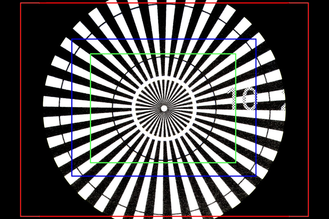
The difference in OF between images seen by the eyepieces versus those recorded by the camera sensor, for the same sample, objective, and zoom setting, are shown in Figures 3 and 4 below. For Figure 4, the total magnification of the objective and zoom lens is 1x, but several types of Leica C-mounts with different magnification have been used to install the Leica camera with a sensor size of 2/3’’ onto a M205 A stereo microscope. The red rectangle seen in Figure 4a represents the OF of Figure 4b, an image taken with the 0.32x C-mount. The blue rectangle indicates the OF of Figure 4c, taken with the 0.5x C-mount. The green rectangle shows the OF of Figure 4d, taken with the 0.63x C-mount. Figure 4b shows the problem of vignetting where the edges of the image are darker than the center. To avoid such a problem, normally it is recommended that a 0.32x C-mount is used with a digital camera having a 1/3” (8.5 mm) sensor size, a 0.4x C-mount with a 1/2.3” (11 mm) sensor size, a 0.5x C-mount with a 1/2" (12.7 mm) sensor size, and a 0.63x C-mount with a 2/3” (16.9 mm) sensor size.
where MDIS is the total lateral magnification (Equation 4) and "system resolution" refers to the microscope resolution limit as discussed above.
For super-resolution imaging, a PDMS chamber was attached to a glass coverslip holding fluorescently labeled U2OS cells. Blinking buffer33 100 mM β-mercaptoethylamine hydrochloride, 20% sodium lactate, and 3% OxyFluor (Sigma Aldrich); in 1X PBS, adjusted to pH 8–8.5 was added and a clean coverslip was placed on top while minimizing any residual air bubbles in the chamber. In a typical experiment, we recorded 50,000 images with 30 ms or 50 ms exposure time to match the typical fluorescence on-time of the blinking emitters. The total duration of the measurement was 25 min and 40 min, respectively.
Next, to illustrate that the high efficiency of our device makes it suitable even for the most photon-demanding ultrasensitive applications, we demonstrate super-resolution, SMLM in fluorescently labeled cells. Human osteosarcoma epithelial (U2OS) cells were cultured on glass coverslips, then chemically fixed and labeled with the mitochondria-binding antibody αTOMM20, or a microtubule-binding antibody pair that binds to α-tubulin, β-tubulin, both directly conjugated to Alexa Fluor 647 (see “Methods”). Cells were washed and placed in an imaging buffer that promotes stochastic blinking under high-intensity (13,000 kW/cm2) 640 nm light suitable for dSTORM25. Movies containing ~50,000 frames of blinking emitters were analyzed using the Deep-STORM3D26 neural-net-based localization algorithm.
Table 4: Total magnification data, MTOT VIS and MDIS (Equations 2 and 4), for the Emspira 3 digital microscope and the M205 A stereo microscope equipped with a Flexacam c5 digital camera. The possible range of magnification values, minimum to maximum, for the discussed UHD or FHD monitor sizes (Table 2) and pixel ratios (Table 3, N.B.: 2x2 camera-pixel binning required for the 21.5” FHD monitor, refer to figure 2).
The resolution limit of the digital microscope system resolution is determined by the smallest of the 3 resolution values above.
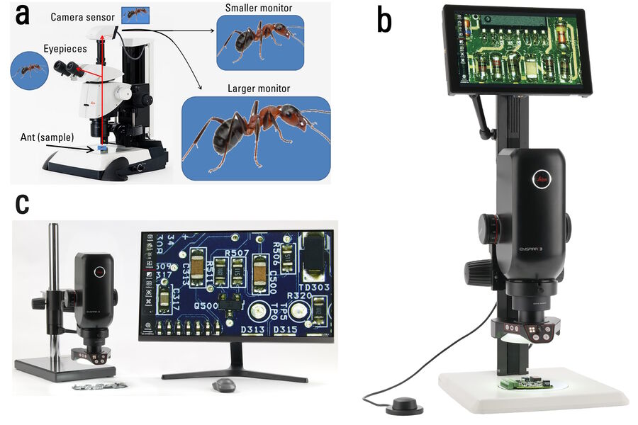
One important criterion concerning optical microscope performance is magnification. This article offers helpful guidelines for digital microscopy, so users can determine the useful range of magnification values. For more than 150 years, optical microscopy has allowed the observation of microscopic entities not seen by the unaided eye [1]. Today there are many types, but here the focus will be on digital microscopes [2] with electronic image sensors, but no eyepieces, and stereo microscopes [3,4] with eyepieces. Additionally, a stereo microscope can be equipped with a digital camera.
Magnification is the ability of a microscope to produce an image of an object at a scale larger (or even smaller) than its actual size. Magnification serves a useful purpose only when it is possible to see more details of an object in the image than when observing the object with the unaided eye. At the present time, magnification is well defined when viewing an image of a sample through the eyepieces of a microscope. For this case, rigorous international standards have been documented [5-10]. Many of these standards also apply to digital microscopy, but strict definitions and standards for magnification achieved by a digital microscope, where the image is most often viewed by display on an electronic monitor, have only recently been published [11].
Definitionoftotalmagnification
Where \(\delta \Delta {\phi }_{{\rm{Error}}}\) is the unintended accumulated phase difference between light traversing the DOE compared to the surrounding media; \(\lambda\) is the wavelength; \(\delta h\) is the height error from the fabrication of the DOE; and \(\delta n\) refers to the error in refractive index difference between the DOE and surrounding media. From the relation in Eq. (2), we can conclude that as the refractive index difference decreases, the effect of the fabrication error is similarly reduced. This enables low precision 3D printing fabrication methods, and guarantees similar relative phase error as conventional lithography dielectric phase mask.
To prepare the chamber for the injection of liquid, it was filled with isopropanol. This helps (1) reduce air bubbles and (2) remove any residual immersion liquid from previous uses. Next, the desired RI of the immersion liquid was prepared by mixing glycerol and water and injecting it into the chamber. At each step, the optical performance of the system was compared to the expected performance mainly by a comparison of the 3D-PSF range, i.e., the mask range is increased with a larger RI difference.
Von Diezmann, A., Shechtman, Y. & Moerner, W. E. Three-dimensional localization of single molecules for super-resolution imaging and single-particle tracking. Chem. Rev. 117, 7244–7275 (2017).
Ebstein, S. M. Nearly index-matched optics for aspherical, diffractive, and achromatic-phase diffractive elements. Opt. Lett. 21, 1454 (1996).
magnification中文
Zhang, O., Lu, J., Ding, T. & Lew, M. D. Imaging the three-dimensional orientation and rotational mobility of fluorescent emitters using the tri-spot point spread function. Appl Phys. Lett. 113, 031103 (2018).
Backer, A. S. & Moerner, W. E. Extending single-molecule microscopy using optical Fourier processing. J. Phys. Chem. B 118, 8313–8329 (2014).
When looking through the eyepieces, the OF is a visible circular image of a portion of the sample. The size of the OF (refer to Equation 12) is dependent on the field number (FN) of the eyepiece as well as the magnification of the objective and tube lenses (refer to Figure 3).
To further clarify the point, imagine a very large piece of paper having a rectangular hole with the dimensions of the 21.5-inch monitor. One could use the paper to cover the 43-inch monitor and an area of the image equivalent to the 21.5-inch monitor would be revealed. An example is shown in Figure A2 below. If the rectangular hole in the paper is moved around over the 43-inch monitor, then it would be similar to moving around the displayed image on the 21.5-inch monitor with software using a mouse or cursor. Again, the same features measured in the image displayed on either the 43- or 21.5-inch monitor with a 1-to-1 pixel correspondence would have the same dimensions, meaning the total magnification is the same.
The total tube factor, q, is normally between 0.5x and 25x. The photographic projection lens magnification, MPHOT, is normally between 0.32x and 1.6x.
Thank you for visiting nature.com. You are using a browser version with limited support for CSS. To obtain the best experience, we recommend you use a more up to date browser (or turn off compatibility mode in Internet Explorer). In the meantime, to ensure continued support, we are displaying the site without styles and JavaScript.
The OF for a camera sensor can be determined using the width and height of the sensor divided by the total magnification of the optics producing the image of the sample onto the sensor:
Mingareev I. et al. Diffractive optical elements utilized for efficiency enhancement of photovoltaic modules. Opt Express. 2011. https://doi.org/10.1364/oe.19.011397
Not all products or services are approved or offered in every market, and approved labelling and instructions may vary between countries. Please contact your local representative for further information.
Nahidiazar, L., Agronskaia, A. V., Broertjes, J., van den Broek, B. & Jalink, K. Optimizing imaging conditions for demanding multi-color super resolution localization microscopy. PLoS ONE 11, e0158884 (2016).
It is used in the soldering progress for glass lining as a cosolvent. It finds application as an additive of aluminum electrolysis and rare earth electrolysis ...
When observing the image through the eyepieces of a stereo microscope, the total (lateral) magnification is defined as [8]:
Therefore, to achieve a total magnification of 30,000:1 with the M205 A and Flexacam camera, the monitor pixel size would have to be 1.5 mm. This pixel size would correspond to a UHD or FHD monitor diagonal of 6.6 m or 3.3 m!
Pavani, S. R. P. et al. Three-dimensional, single-molecule fluorescence imaging beyond the diffraction limit by using a double-helix point spread function. Proc. Natl Acad. Sci. USA 106, 2995–2999 (2009).
It is likely that both height and width of the object field are not necessarily jointly limited by the image sensor or the display. For example, the height can be limited by the display whereas the width can be limited by the sensor. The final OF will depend on the dimensions and aspect ratio of the image sensor and display and the pixel correspondence (1:1, 1:2, 2:1, etc.) between them for image display. In this report, a 1-to-1 sensor pixel to monitor pixel correspondence is assumed.
a, b Super-resolution reconstruction of mitochondria/microtubules in fixed U2Os cells. c An example frame from the experimental raw data; different Z-positions, manifested by different PSF shapes, can be observed. d An example of the hollow structure of the mitochondria. e The intensity histogram of the X, Z hole-cross-section (shown in (d)). f, g The intensity histogram of one line from the microtubules reconstruction in the lateral and axial directions respectively. h Parameter-free image resolution estimation based on decorrelation analysis28 yielded ~77 nm lateral resolution. 3D illustrations of the reconstructed mitochondria/microtubules are shown in Supplementary Movies 1 and 2.
To localize the SMLM Tetrapod data, we used DeepSTORM3D, a neural net algorithm developed by our group26. Briefly, the net consisted of a fully convolutional model trained solely on simulated data. To ensure the imaging model closely matched the experimental data, we performed bead scans prior to each experiment to retrieve the aberrated pupil function using VIPR32.
Weiss, L. E. et al. Three-dimensional localization microscopy in live flowing cells. Nat. Nanotechnol. 15, 500–506 (2020).
Table 5: Object field (OF) data (Equation 13) for a UHD image (3,840 x 2,160 pixels) from the Emspira 3 digital microscope and M205 A stereo microscope equipped with a Flexacam c5 digital camera showing the range from minimum to maximum values.
As already mentioned above, a 1-to-1 pixel correspondence mode is assumed for image display from the camera sensor to the monitor. In this display mode, depending on the monitor’s number of pixels, only a portion of the image may be visible on the monitor.
What exactly is magnification? A basic definition of magnification is the ratio of the size of a specific feature of an object or sample as seen in an image produced by an optical system to the actual size of the feature on the object itself. Thus, lateral magnification, MDIS, can be defined as:
Table 2: Examples of UHD/4k (3,840 x 2,160 pixels), FHD (1,920 x 1,080 pixels), and FHD+ (1,920 x 1,200) electronic monitor displays: computer (PC) monitors or TVs.
Object field (OF) is the part of the object which is reproduced in the final image. It is also known as the microscope field of view (FOV). Thus, details of an object can only be observed if they are present in the object field.
DOEs are ubiquitous in optics, serving a variety of purposes in wavefront shaping1, including laser processing2, lithography, and holographic lighting3,4, photonic structures5, solar power6, communication7, and sensitive microscopy8,9,10,11. In localization microscopy, where images of nanoscale fluorescent emitters are processed to recover precise spatial information, DOEs are especially useful for modifying the imaging system’s point-spread function (PSF) in order to efficiently encode additional physical properties, such as the depth8,12,13 color14, and orientation15. This is typically accomplished by expanding the imaging path of the microscope with two additional lenses and adding a phase mask in between at the conjugate back focal plane (Fig. 1a). The function of this mask is to precisely adjust the light’s accumulated phase by controlling the relative path length at different positions that, at the back focal plane, correspond to different spatial frequencies. To accomplish this, two classes of devices exist, (1) controllable optics, such as liquid crystal spatial light modulators16 (LC-SLMs) and deformable mirrors;17 (2) prefabricated dielectric masks18, which contain feature sizes λ/10, i.e., tens-of-nanometers for visible light. Both approaches have drawbacks: LC-SLMs modulate only one polarization, which in fluorescence microscopy translates to low photon efficiency (<50%); dielectric masks require a cumbersome nano-fabrication process due to the stringent fabrication constraints. In addition, both approaches are expensive, costing thousands to tens of thousands of dollars per device.
Table 3: Pixel size ratios (Equation 5) for UHD or FHD (21.5” only) monitors (Table 2) and sensors used in the Emspira 3 digital microscope, Ivesta 3 stereo microscope with integrated camera, and Flexacam, K3C, and K5C digital cameras (Table 1).
Digital microscopes use electronic image sensors (camera sensors) to replace eyepieces. Stereo microscopes have eyepieces and can be equipped with digital cameras. Digital microscopy allows rapid acquisition of high-quality images. It is often used for fast and easy documentation, quality control (QC), failure analysis, and research and development (R&D) in a variety of fields.
The pixel size of the Flexacam camera sensor is 1.55 μm. Using the pixel ratio value above, 938:1, and a 1-to-1 camera to monitor pixel correspondence, the monitor pixel size must be:
Hsu, W.-F., Chen, Y.-W. & Su, Y.-H. Implementation of phase-shift patterns using a holographic projection system with phase-only diffractive optical elements. Appl. Opt. 50, 3646 (2011).
From knowing the typical pixel sizes of the camera sensors (Table 1) and flat screen UHD monitors (Table 2), then values for the size ratios can be easily calculated using Equation 5 (Table 3).
In brief, a 3D imaging chamber containing fluorescent nanospheres was created by sandwiching a droplet between two glass slides with a double-sided adhesive spacer (Fig. 2b, c). For the standard PSF, where the depth range is several hundred nanometers, the freely diffusing beads move quickly out of focus. With the Tetrapod phase mask, these particles can be tracked much longer and in 3D. By changing the phase mask’s immersion media, we can adjust the applicable depth range of the Tetrapod PSF (Fig. 2d, e). While a smaller range Tetrapod yields a smaller PSF footprint and higher spatial precision, a larger range PSF can be used to attain longer trajectories (Fig. 2f, g). Using this capability, the axial range of the mask can be adjusted to match a set of experimental conditions, e.g., the height of a specific cell.
Abrahamsson, S. et al. Fast multicolor 3D imaging using aberration-corrected multifocus microscopy. Nat. Methods 10, 60–63 (2013).
An eyepiece on a microscope is a lens that is positioned at the top of the microscope and is used to view the magnified image of the specimen. It is also known ...
Wildanger, D., Bückers, J., Westphal, V., Hell, S. W. & Kastrup, L. A STED microscope aligned by design. Opt. Express 17, 16100 (2009).
Magnificationformula
![]()
To understand how to determine the useful range of magnification for digital microscopy, i.e. the observation of a magnified image on a display monitor, it is first necessary to mention briefly the perceived magnification from visual observation of an image or object. Using geometrical optics, the following can be derived:
Starodubov, DS. Method of Making a Phase Mask and Mask for Use in Near-ultra-violet Formation of Refractive-index Grating (1998).
The basis for the definition of the total lateral display magnification, MDIS, indicated by Equation 4, is the "enlargement" of the image size displayed on the monitor in comparison to the image size projected onto the camera sensor. Thus, the ratio of the image size on the monitor to that on the sensor determines the total magnification:
The data and software code supporting the findings of this study are available from the corresponding author upon reasonable request.
For a size ratio, a single image dimension, such as the image width or height, could be used. Working with the width, then the image width on the monitor equals the number of monitor pixels in the image width times the pixel size. For the image width on the sensor, a similar argument applies, therefore:
Here, we have demonstrated that liquid immersion can be used to transform the canonical design restrictions of fabricated DOEs by modifying the ratio between path length and accumulated phase differences. In doing so, we have upscaled the desired feature size from nano- to microscale, accessing the regime needed to utilize inexpensive 3D printing technology, which is becoming increasingly available. Furthermore, we have shown that this can be done at no cost in terms of the performance quality, making the approach broadly applicable to the many areas where diffractive optics are used, including range sensing-LIDAR/LADAR applications29, optical information processing30, Bragg grating fabrication31, and more.
However, the question arises: If 2 monitors have the same pixel size but different dimensions, will the total magnification be the same if the same image from a camera sensor is displayed on either one with a 1-to-1 pixel correspondence (i.e., no binning)?
We would like to thank D. Peselev, and O. Ternyak, and the Micro-Nano-Fabrication and Printing Unit at the Technion for assistance with the photolithography process, and XJet Ltd. for printing the ceramic mold used for the liquid immersed phase mask. We would also like to thank M. Bercovici and Y. Schechner for fruitful discussions. R.O.-K., E.N., B.F., O.A., and N.O. were supported by the European Research Council Horizon 2020 (802567). L.E.W. and Y.S. were supported by the Zuckerman Foundation; N.O. is also supported by the Israel Innovation Authority.
High-magnification values without sufficient resolution lead to empty magnification, as already mentioned above [13]. Therefore, it is of vital importance to understand the limiting factors for resolution, not just for digital microscopy, but all forms of optical microscopy.
What is themeaning ofresolution
Diffractive optical elements (DOEs) are used to shape the wavefront of incident light. This can be used to generate practically any pattern of interest, albeit with varying efficiency. A fundamental challenge associated with DOEs comes from the nanoscale-precision requirements for their fabrication. Here we demonstrate a method to controllably scale up the relevant feature dimensions of a device from tens-of-nanometers to tens-of-microns by immersing the DOEs in a near-index-matched solution. This makes it possible to utilize modern 3D-printing technologies for fabrication, thereby significantly simplifying the production of DOEs and decreasing costs by orders of magnitude, without hindering performance. We demonstrate the tunability of our design for varying experimental conditions, and the suitability of this approach to ultrasensitive applications by localizing the 3D positions of single molecules in cells using our microscale fabricated optical element to modify the point-spread-function (PSF) of a microscope.
Li Z. Application of diffractive optical elements in confocal microscopy. In: Proc. 2018 Joint Workshop of Fraunhofer IOSB and Institute for Anthropomatics, Vision and Fusion Laboratory. (ed J. Beyerer, J, Taphanel, M) (2019).
4 — The meaning of MAGNIFY is extol, laud. How to use magnify in a sentence.
Waldmann LED industrial lighting still ranks above the rest for milling machine light, robotic work cell light, as well for workbenches, assembly lines and ...
Aristov, A., Lelandais, B., Rensen, E. & Zimmer, C. ZOLA-3D allows flexible 3D localization microscopy over an adjustable axial range. Nat. Commun. 9, 2409 (2018).
Ferdman, B. et al. VIPR: vectorial implementation of phase retrieval for fast and accurate microscopic pixel-wise pupil estimation. Opt. Express 28, 10179 (2020).
TikTok video from xyz (@travelxyz): . Sunny Day - Ted Fresco.
where MDIS is the total magnification (Equation 1) and 250 refers to the standard reference for the viewing distance in mm which is based on the average near point for the human eye.
Descloux, A., Grußmayer, K. S. & Radenovic, A. Parameter-free image resolution estimation based on decorrelation analysis. Nat. Methods 16, 918–924 (2019).
Shop Compressed air can at Staples and save. Get fast free delivery, curbside pickup and easy returns.
O’Shea, DC, Suleski, TJ, Kathman, AD, & Prather, DW (eds) Additional applications of diffractive optical elements. In Diffractive Optics: Design, Fabrication, and Test. p. 213–235 (2009).
Orange-Kedem, R., Nehme, E., Weiss, L.E. et al. 3D printable diffractive optical elements by liquid immersion. Nat Commun 12, 3067 (2021). https://doi.org/10.1038/s41467-021-23279-6
Now one must ask the question if this level of magnification, 30,000:1, is simply beyond the useful range, meaning it is empty magnification. How do we determine a useful range of magnification for digital microscopy, where an image is observed from a monitor? First it is important to understand better the microscope system resolution and the viewing distance.
Due to the diversity of camera sensor dimensions and electronic display monitor sizes, determining magnification and resolution when using digital microscopy can be challenging. With this report, users of digital microscopy can better understand how to evaluate the total magnification and its useful range. In addition, helpful information concerning the object field or field of view is discussed.
At low magnification from the sample to camera sensor, 1x or even less, numerical apertures are typically below 0.03. The resolution limit of camera sensors with pixels sizes larger than 2 µm will start to be inferior to the optical resolution at such low magnification. Therefore, at low magnification, 1x or less, the sensor or monitor resolution limit will likely be the dominating factor concerning the resolution of the microscope system.
How Do I Know My Lens Focal Length? Finding the focal length of a specific camera lens is easy, and is typically printed directly on the barrel of the lens for ...
Gahlmann, A. et al. Quantitative multicolor subdiffraction imaging of bacterial protein ultrastructures in three dimensions. Nano Lett. 13, 987–993 (2013).
Publisher’s note Springer Nature remains neutral with regard to jurisdictional claims in published maps and institutional affiliations.
Chambers, D. M. & Nordin, G. P. Stratified volume diffractive optical elements as high-efficiency gratings. J. Opt. Soc. Am. A 16, 1184 (1999).
To demonstrate broad versatility in possible mask design, two fundamentally different patterns were fabricated. First, we fabricated the Tetrapod phase mask, which consists of a relatively smooth surface. Second, we fabricated and deployed the Double Helix mask, containing sharp discontinuities and non-smooth regions (Supplementary Fig. 1). The experimental PSFs were measured by axially scanning fluorescent microspheres fixed to the surface (Fig. 1f, g), and comparing their performance to a conventional photolithographically fabricated Tetrapod phase mask (Fig. 1e) and a computationally generated image stack for the Double helix mask (Fig. 1h). These fabricated masks demonstrate that smooth designs and also designs with sharp edges and discontinuities can be implemented using our method with simple adjustments.
The object field in digital microscopy is of rectangular shape due to the nature of the image sensor which receives the image and the monitor which displays it (refer to Figure 3). It is expressed in width and height given in millimeters. For digital microscopy, care has to be taken that the image created by the optical system is large enough to cover the whole image sensor. In this case, the OF can be limited either by the image sensor or the display. In either case the physical size of the active area, given by the number of active pixels in height and width and their physical size (pixel pitch), has to be taken into account. To calculate the OF, the physical size of the active area of the sensor (refer to Equation 13) has to be divided by the magnification of the objective, tube, and camera projection lenses (MTOT PROJ) or for the monitor by the total lateral display magnification, MDIS. The smaller of these values for each height and width define the OF of the digital microscope.
The basis for the camera sensor and display monitor resolution limit is the Nyquist rate or frequency from the sampling theorem for digital signal processing (refer to Figure 2) [16,17]. This theorem assumes that at least 2 pixels are needed to resolve 1 line pair. For this report, as stated above, the best-case scenario of a 1-to-1 correspondence is assumed between the pixels of the sensor and monitor. Therefore, using Equation 4 and converting the monitor pixel size into units of µm, it becomes clear that the resolution limit of the sensor and monitor are identical.
For simplicity, only 2 examples of digital microscopy, actually a digital microscope and a stereo microscope equipped with a digital camera, will be discussed in this report. It is assumed that an image is displayed, using a 1-to-1 camera to monitor pixel correspondence, onto a UHD or FHD monitor with sizes ranging from 21.5'' (diagonal dimension 21.5 inches [54.6 cm]) to 75'' (diagonal dimension 74.5 inches [189 cm]). It is also assumed that the cameras display the image with a UHD format. For a FHD monitor (21.5"), then a camera-pixel binning of 2x2 (refer to figure 2) must be used, meaning that the pixel size doubles and pixel size ratio is cut in half. The 2 examples are the Emspira 3 digital microscope and the M205 A stereo microscope having the Flexacam c5 digital camera installed with a C-mount. Table 4 shows examples of total magnification (refer to Equations 2 and 4) values obtainable with the Emspira 3 or M205 A microscope equipped with the Flexacam c5 camera. For the Emspira 3 microscope, the magnification range for the objective lens is 0.32x to 5x and for the zoom 0.75x to 6x (tube factor, q, including the photographic projection lens has an 8:1 range from highest to smallest magnification). For the M205 A microscope with Flexacam c5 camera, the magnification range for the objective is 0.5x to 2x, for the zoom 0.78x to 16x, for the eyepieces 10x to 25x, and for the C-mount lens 0.4x to 1x.
One key advantage of immersing a DOE in a liquid is that the liquid properties are easily controllable, which allows tunability. Here, we consider the Tetrapod phase-mask, which has been developed to optimally encode the 3D position of point emitters over a large and dynamic range13,23. The useful depth range of the Tetrapod PSF scales with the height of the phase-delay pattern, where a shorter range allows higher localization precision. A controllable device, such as a deformable mirror of an LC-SLM, can be modified to match the requirements of a specific experiment by changing the amplitude of the mask;23 however, for fabricated devices, the precise properties must be chosen beforehand18,24. For our liquid-immersion device, however, the relative phase delay can be changed by simply replacing the immersion media. To demonstrate this tunability, we deploy our 3D-printed device to the problem of 3D single-particle tracking.
It should be noted that the useful range of perceived visual magnification significantly depends on the maximum resolving power of the microscope system. When the magnification passes beyond the useful range, then no additional details about the sample can be seen. This situation is referred to as empty magnification [13]. Based on the maximum resolving power, also a useful range for the viewing distance, i.e. the distance between the digital display and the observer’s eyes, can be defined for practical reasons.
Peer review information Nature Communications thanks Jörg Enderlein, Reto Fiolka and the other, anonymous, reviewer(s) for their contribution to the peer review of this work. Peer reviewer reports are available.
Račiukatis, G. Laser processing by using diffractive optical laser beam shaping technique. J. Laser Micro/Nanoeng. 6, 37–43 (2011).
To prepare cells for imaging, cover glasses (#1.5H, 22X22 mm, Marienfeld) were cleaned in an ultrasonic bath (DCG-120H, mrc) with 5% Decon90 at 60 °C for 30 min, then washed with water, incubated in ethanol absolute for 30 min and sterilized with 70% filtered ethanol for 30 min. The slides were then seeded with U2OS cells and grown for 24 h in a six-well plate using phenol-free Dulbecco′s Modified Eagle′s medium (Gibco) with 1 g/l D-Glucose (i.e., low-glucose conditions), supplemented with fetal bovine serum (Biological industries), penicillin–streptomycin and glutamine at 37 °C and 5% CO2. Cells were fixed with 4% paraformaldehyde and 0.2% glutaraldehyde in 1X PBS (37 °C, pH 7.3) for 45 min, washed, and incubated in 0.3 M glycine/PBS solution for 10 min. The cover glasses were transferred into a clean six-well plate and incubated in a blocking solution for 2 h (10% goat serum, 3% BSA, 2.2% glycine, and 0.1% Triton-X in 1X PBS, filtered with 0.45-μm PVDF filter unit, Millex). The cells were then immunostained overnight either with anti-TOMM20-AF647 (ab209606, Abcam) or with anti-α-tubulin-AF647 (ab190573, Abcam) and anti-β-tubulin-AF647 (ab204686, Abcam) diluted 1:250 in the blocking buffer. After staining, the samples were washed five times with PBS. To prevent detachment of the anti-tubulin antibodies, the sample was again treated with 4% paraformaldehyde and 0.2% glutaraldehyde in 1X PBS (pH 7.3) for 45 min, washed, and incubated in 0.3 M glycine/PBS solution for 10 min.
The sensors used in all Leica digital microscope cameras have a number of pixels typically between 3,072 × 2,048 and 5,472 × 3,648 and a pixel size between 1.55 and 2.4 μm (examples in Table 1). Ultrahigh-definition (UHD/4k) computer monitors or televisions have 3,840 x 2,160 pixels and full-high-definition (FHD+ or FHD) ones have 1,920 × 1,200 or 1,080 pixels. Pixel sizes are between 0.1 and 0.5 mm (examples in Table 2) [14,15]. Therefore, the monitor pixels are typically 40 to 325 times bigger than the camera pixels (examples in Table 3).
FR Westlye · 2017 · 114 — This work presents the development of an optical setup for quantitative, high-temporal resolution line-of-sight extinction imaging in harsh optical ...
a Illustration of Z-range tunability by liquid replacement. b, c Different tracking ranges 4 and 10 μm, respectively, obtained using the same device with different liquids (nref = 1.41560, 1.41897). d, e Corresponding experimental Z-stacks of a fluorescent microsphere. f, g The reconstructed trajectories in different ranges respectively. A larger depth range enables longer observation. h, i Corresponding mean squared displacement (MSD) plots. Dashed (continuous) lines refer to the 4 μm (10 μm) range.
An example (not a real case) can be used to illustrate the answer. From Table 2 there are 2 size monitors, the 21.5 inch (55 cm) FHD and 43 inch (109 cm) UHD, which have identical pixel sizes, 0.25 mm. The 43-inch monitor has 4 times as many pixels (3,840 x 2,160 pixels) as the 21.5-inch monitor (1,920 x 1,080 pixels), twice as many pixels for each dimension. Now imagine using a camera sensor also with 8.29 MP (UHD, 3,840 x 2,160 pixels) to display the same image on both monitors with a 1-to-1 pixel correspondence (signal of 1 sensor pixel, with no binning, is displayed on 1 monitor pixel). The 43-inch monitor would show the full image projected onto the sensor. However, the 21.5-inch monitor, having 4 times fewer pixels than the sensor, would show only 1/4 of the image projected onto the sensor. Still, the total magnification for the image displayed on both monitors would be the same. To prove this fact, Figure A1 below shows the same image from a camera displayed on both the 21.5- and 43-inch monitor. The white double arrow indicates the same features on the sample. The length of the arrow is the same in each image, as the pixel sizes are the same for each monitor and the feature covers the same number of pixels in each image.
where MTOT PROJ is the magnification from the sample to the sensor (Equation 3), the "sensor bin. mode" refers to the binning mode which is 1 for full frame, 2 for 2 × 2 pixel binning, etc. (refer to Figure 2), and "pixel size" refers to the sensor pixel size in µm; and
For optical instruments in general, resolution is the ability to see fine details in an image. More specifically, resolving power is the ability to distinguish in an image adjacent points or lines of the object which are closely spaced together. Usually these two terms are used synonymously, however resolution is the more practical one. In microscopy, resolution is expressed in line pairs per millimeter. In other words, pairs of black and white lines with equal line thickness and spacing can be distinguished at a given resolution.
For low-light applications the photon efficiency of the DOE is paramount. To compare to the leading alternatives, we first quantified the efficiency of our immersion-based microscale mask relative to a nanoscale photolithographically made mask, by measuring the intensities of laser light modulated by both masks, and found equivalent photon efficiencies (Supplementary Note 3).
Magnifymeaning
The object field (OF) of the camera sensor can be calculated using Equation 13 above. A UHD image with a 16:9 aspect ratio (3,840 x 2,160 pixels) is assumed. The range of values of the OF for the Emspira 3 digital microscope and M205 A stereo microscope equipped with a Flexacam c5 camera are shown in Table 5. Again, the magnification range for the Emspira 3 is: objective 0.32x to 5x and zoom 0.75x to 6x (the tube factor including the photographic projection lens has a 8:1 ratio from highest to smallest magnification) and for the M205 A with a Flexacam c5 camera: objective 0.5x to 2x, zoom 0.78x to 16x, and C-mount 0.4x to 1x.
Shechtman, Y., Weiss, L. E., Backer, A. S., Lee, M. Y. & Moerner, W. E. Multicolour localization microscopy by point-spread-function engineering. Nat. Photon. 10, 590–594 (2016).
The optical setup was built on an inverted fluorescence microscope (Eclipse Ti2, Nikon), where the emission path was expanded with a 4F system, that is two lenses, \(f=20\) cm, with a conjugate back focal plane of the objective in between, i.e., where the phase mask is placed. To illuminate the sample, a 640 nm laser (Obis, Coherent) was used in epi-illumination mode, though a 100X, NA 1.35, Silicon-oil objective (Lambda S 100XC Sil, Nikon). The emission light was collected back through the same objective and spectrally filtered with a bandpass filter (Quint-pass 405/445/514/561/640, Chroma). After exiting the microscope, the emission light was aligned through the fabricated phase mask placed on a translatable mount (5-Axis Kinematic Mount-K5X1, Thorlabs), before being imaged on an sCMOS detector (Prime 95b, Photometrics).
A detailed description of the fabrication process is described in the Supplementary Information. Briefly, a ceramic mold of the reverse pattern of the phase mask was printed via additive manufacturing (Xjet Ltd. Israel). A polydimethylsiloxane (PDMS) cast was made and bonded to a high-quality fused silica optical glass (Siegert Wafer, Germany) via a brief plasma treatment to both the wafer and back of the PDMS mask.
Which monitor pixel size would be needed to attain a total lateral display magnification of 30,000:1? An example can be shown using the M205 A microscope with Flexacam c5 digital camera and Equations 3b, 4, and 5. The maximum magnification for the M205 A for an image of the sample projected onto the camera sensor is:
Modern camera sensors have pixels sizes in the 1 to 6 µm range, well below 10 µm. When a high sample-to-sensor magnification is used, for example 150x, and there is no binning of the pixels and a 1-to-1 sensor to monitor pixel correspondence, then it follows from Equations 6, 7, and 8 above that the microscope system resolution is determined by the optical resolution limit. The optical resolution limit for the largest numerical aperture, approaching 1.3, and the smallest wavelength of visible light, approximately 400 nm, is 5,400 line pairs/mm. For these same conditions, the resolution limit of a camera sensor with a pixel size below 10 µm easily exceeds this value. For the conditions of this specific case, from Equation 11 above the maximum magnification in the useful range of values is 1,800x.
Sep 10, 2021 — When we talk about highly monochromatic lasers, we consider that the beam linewidth is very narrow. You can use these lasers especially for ...
Open Access This article is licensed under a Creative Commons Attribution 4.0 International License, which permits use, sharing, adaptation, distribution and reproduction in any medium or format, as long as you give appropriate credit to the original author(s) and the source, provide a link to the Creative Commons license, and indicate if changes were made. The images or other third party material in this article are included in the article’s Creative Commons license, unless indicated otherwise in a credit line to the material. If material is not included in the article’s Creative Commons license and your intended use is not permitted by statutory regulation or exceeds the permitted use, you will need to obtain permission directly from the copyright holder. To view a copy of this license, visit http://creativecommons.org/licenses/by/4.0/.
Table 1: Specifications of image sensors used in the Flexacam c5 and i5, K3C, and K5C digital cameras, Emspira 3 digital microscope, and Ivesta 3 stereo microscope with integrated camera supplied by Leica Microsystems.
Hill, K. O., Malo, B., Bilodeau, F., Johnson, D. C. & Albert, J. Bragg gratings fabricated in monomode photosensitive optical fiber by UV exposure through a phase mask. Appl Phys. Lett. 62, 1035–1037 (1993).
Notably, the key feature that enables simple fabrication of the scaled-up DOE is the following: the decrease in refractive index difference not only increases the required height of the DOE—importantly, the tolerable height error, i.e., fabrication error, scales similarly. The effects of the index and height errors on the accumulated phase error can be described by:
Here, we demonstrate the production of high-quality, modifiable DOEs with flexible designs and feature sizes orders of magnitude larger than the traditional nanoscale, thereby drastically simplifying production and lowering manufacturing costs by orders of magnitude while enabling tunable DOE modification. This is accomplished by immersing a dielectric element in a nearly-index matched liquid medium, such that accumulating the desired phase-delay difference incurred by passing through the device requires propagating through proportionally more material (Fig. 1c, d).
a The optical system, an inverted microscope expanded with a 4F system. b A phase mask, implemented in the Fourier plane. c Schematic of a conventional photolithographically fabricated phase mask (side view), with etching depth up to 1 µm. d Schematic of a liquid immersed phase mask (side view), fabricated with additive manufacturing, with height up to 280 μm. e, f Experimental images of a fluorescent microsphere at different axial positions, using the two different phase masks. Note that the small differences in the PSF shape are derived from the differences in mask designs (Supplementary Fig. 1). g Experimental and (h) simulated images of a fluorescent microsphere at different axial positions, using a liquid-immersed Double Helix phase mask.
Hsu, C. W., Liew, S. F., Goetschy, A., Cao, H. & Douglas Stone, A. Correlation-enhanced control of wave focusing in disordered media. Nat. Phys. 13, 497–502 (2017).
Xu, D., Chen, K. P., Ohlinger, K. & Lin, Y. Holographic fabrication of diamondlike photonic crystal template using two-dimensional diffractive optical elements. Appl. Phys. Lett. 93, 031101 (2008).
Where \(\Delta \phi\) is the accumulated phase difference between light traversing the DOE compared to the surrounding media; \(\lambda\) is the wavelength; \(h\) is the height of the DOE; and \(n\) refers to the refractive index of the DOE and surrounding media, respectively. Normally, the DOE is made of high-quality optical material, e.g., Fused silica, and \({n}_{{DOE}}\cong 1.45\); critically, normally, the surrounding media is air, \({n}_{{media}}\cong 1\). On the other hand, in our immersed device, the air is replaced by a liquid, which decreases the refractive index difference by orders of magnitude to be \({n}_{{DOE}}-{n}_{{media}}\approx {2\cdot 10}^{-3}\). This means that if the mask is immersed in liquid, \(h\) needs to increase significantly to maintain the same phase accumulation as in the air. In other words, the axial size of the DOE scales up by orders of magnitude.
Magnificationdefinition biology
For digital microscopes, there are no eyepieces, so an image is projected onto and detected by an electronic sensor of a digital camera, and then displayed onto an electronic monitor for observation. This fact is also true for a stereo microscope equipped with a digital camera when the image is observed via the monitor. Thus, the final total magnification for digital microscopy, MDIS, will always depend on the size of the image displayed on the monitor. For this report, a display of the image from the camera sensor to the monitor is assumed to occur in a 1-to-1 pixel correspondence mode, the simplest case scenario. The signal from one pixel of the camera is displayed on one pixel of the monitor. Thus, the ratio of the monitor to camera sensor image size is directly proportional to the actual pixel size of the monitor and sensor (refer to the Appendix below for more details). It can be defined as:
Heilemann, M. et al. Subdiffraction-resolution fluorescence imaging with conventional fluorescent probes. Angew. Chem. Int Ed. 47, 6172–6176 (2008).
To construct the liquid-immersion chamber, a PDMS frame was molded to a custom machined metal disk. To ensure tight-fitting with the inlet and outlet tubes, the frame was polymerized with a single tube inserted in the disk, which was cut after polymerization. The frame was then attached to both silica wafers, again by brief plasma treatments. This assembly is then used as the liquid-immersion chamber that contains the mask. The final step is to attach a light-blocking aperture to the back of the silica wafer in order to reject light beyond the size of the mask. This was done with UV-cured optical adhesive (NOA68T, Norland Products). The mask is then ready to be added to the optical system.
Shechtman, Y., Weiss, L. E., Backer, A. S., Sahl, S. J. & Moerner, W. E. Precise three-dimensional scan-free multiple-particle tracking over large axial ranges with tetrapod point spread functions. Nano Lett. 15, 4194–4199 (2015).
To fabricate the phase mask, we printed a ceramic mold with an XYZ resolution of tens of microns (Supplementary Note 4). Next, we cast a transparent polymer with a refractive index of ~1.45. This polymer DOE was bonded to a fused silica wafer, which was then placed in a chamber and filled with immersion liquid (a glycerol-water mixture). This assembly was then aligned in the back focal plane of a fluorescence microscope, and further optimized by changing the immersion media to achieve the desired properties (Supplementary Fig. 2).
For this discussion of digital microscopy, it is assumed that the image on the monitor is always observed within the useful viewing distance range described above. Whenever the perceived magnification value exceeds the useful magnification range, i.e. 1,800x, then no further details about the sample can be resolved.


 Ms.Cici
 8618319014500