
Norland Optical Adhesives - norland adhesive
Expected spectral resolution and simultaneous bandpass are also influenced by how light is coupled into the spectrograph, the central wavelength of interest and associated grating “working angle”, as well as the detector pixel array format at the output plane. Some of these trade-offs can be assessed with the Andor resolution calculator for Kymera and Shamrock Czerny-Turner spectrographs.
Optical microscopy is an ideal method for general inspection purposes, illuminating and producing a magnified image of a specimen. The layout between optical microscopes varies, depending on the application, but generally includes a converging lens (for magnification) and a concave mirror (to aid illumination). The sample is placed on a stage and the resultant image is viewed through an eyepiece.
These influence the choice of grating line density, blaze angle/wavelength, master (different masters for a given line density and blaze angle yield different efficiency and polarisation characteristics) and grating size.
Optical microscopy and electron microscopy both have advantages and disadvantages. SEMs are superior in terms of resolving power and depth of focus. However, optical microscopes are generally easier and quicker to use. As a result, many use a combination of both imaging tools where an optical microscope is used to detect gross defects and SEMs can observe those defects in more detail while observing micro-defects that are not visible using optical microscopy. This two-phase approach combines the benefits associated with each inspection method and provides the customer with a more detailed inspection in less time.
Optical microscopy definition: Optical microscopes use a beam of light, ranging from 400nm to 650nm in wavelength, allowing the observer to analyze the effect of light as it is applied to a specimen.
The human eye is a powerful visual tool but it does not have the resolution to bring microscopic images into focus. This is where microscopy can help us understand everything from pandemic-inducing viruses to the manufacture of increasingly miniaturized electronics, revealing the large impact the smallest detail can have on our day-to-day lives and future endeavors.
Opticalmicroscope working principle
SEMs typically feature three types of detectors, each of which captures a different signal coming from the sample: A Secondary Electron Detector (SED), a Back-Scattered Electron Detector (BSED), and an Energy Dispersive Spectrum Detector (EDS).
In contrast, SEMs can create a three-dimensional appearance of the specimen image. This is because of the method in which the data is obtained, where a fine electron beam is scanned over the surface and the detected secondary electrons form an image with a high depth of focus.
where: n is the order of diffraction, λ is the diffracted wavelength d is the grating constant (the distance between successive grooves) θi is the angle of incidence measured from the normal and θd is the angle of diffraction measured from the normal. The diagram above shows the orders of the diffracted wavelength. As well as positive orders, light can also be diffracted in the opposite direction (i.e. n = -1, -2 etc.) Higher orders may also appear, but these decrease in intensity. Usually the first order lines (n=1 or n=-1) are the most intense.
Many stationary microscopes have several objective lenses that the user can rotate to view the object at varying levels, or powers, of magnification. Now, ...
Harbor Freight buys their top quality tools from the same factories that supply our competitors. We cut out the middleman and pass the savings to you!
In this post, we examine two key methods: optical microscopy and electron microscopy, revealing the benefits each technique brings, and explaining both their differing application areas and operation.
Light microscope diagram
The Andor Shamrock SR-500i imaging spectrometer is based on Czerny-Turner optical design. The optimized optical design provides exceptional performance for multi-track Spectroscopy.…
Edmund Optics lens tissuecommercial grades used in optics and photonics applications are available at Edmund Optics.
Optical microscopesfor sale
This is because, for the optical microscope, the depth of focus is the distance above and below the image plane over which the image appears in focus. As the magnification increases in the optical microscope, the depth of focus decreases.
A diffraction grating is an optical element, which separates (disperses) polychromatic light into its constituent wavelengths (colors). The polychromatic light incident on the grating is dispersed so that each wavelength is reflected from the grating at a slightly different angle. The dispersion arises from the wavefront division and interference of the incident radiation from the periodic structure of the grating.
Opticalmicroscopy in materials Science
SEMs are typically larger and operate in a vacuum, which can increase the time to image a sample. Plus, the resulting image is grey-scaled.

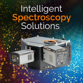
Andor’s new Mechelle ME5000 Echelle spectrograph has been designed to provide simultaneous recording of a wide wavelength range (200-975 nm) in one acquisition. It has no moving…
Shop polarized sunglasses that reduce glare & enhance clarity so you see clearly. Select from stylish designs that provide superior eye ...
The dispersed light is then re-imaged by the spectrograph and the required wavelength range is directed to a detection system. Gratings consist of equally spaced parallel grooves, formed on a reflective coating and deposited on a substrate. The shape of the grooves (blaze angle) influences what wavelength range the grating is best optimised for.
In comparison, SEMs are capable of much greater magnification and higher resolution. The most sophisticated SEMs can achieve magnifications of around 100,000 x and sub-nanometer resolutions, which are capable of imaging viruses (which are between 30 and 250 nm) and molecules such as proteins (10 nm) and glucose (1 nm).
To get the displacement in liters, use a cubic inches to liters conversion calculator. You can also multiply cubic inches by 0.016387 to get the displacement in ...
A ronchi grating is a transparent plate ruled with black lines and equal, clear spaces. It is used as a multiple knife-edge for testing a concave mirr.
Opticalmicroscope uses
Looking at a standard optical microscopy definition, the resolving power of these systems is directly influenced by the wavelength of the imaging beam, which gives SEMs a distinct advantage. Because optical microscopes are limited to the wavelengths of visible light, they can only offer limited magnification (around 1,500 x) and cannot go beyond around 200 nm resolution laterally and 600 to 700 nm axially.
SEM definition: SEMs scan a focused beam of electrons across the surface of a sample, where electromagnets are used to focus the negatively charged electrons. The interaction of the electron beam with the surface of the sample affects the images received. The electrons coming out of the sample are used to create a detailed image and reveal information including the texture (morphology), chemical composition, crystalline structure, and material orientation.
Optical microscopesprice
At Thermo Fisher Scientific, we have decades of cross-sector experience, helping industrial and research users get the best images of the micro world. If you could like to find out more about the best inspection tools for your application, click here to speak to one of our expert teams today.
Sep 30, 2024 — The next notable use of magnifying glasses is fingerprint analysis. Small details and intricate labeling often require scrutiny in laboratory ...
Emission Range: Visible ; Emission Wavelength: 457 nm, 488 nm, 514 nm (Multi-Line) ; Frequency & Mode Operation: Single Transverse Mode ; Laser Class: IIIb ; Noise ...
Andor’s Kymera 193i spectrograph has been designed with research-grade performance, versatility and ease of use in mind. The ‘intelligent’ motorized adaptive focusing allows access…
Types ofoptical microscopes
However, SEMs are gaining ground in this area with many Desktop SEMs bridging the gap between optical microscopes and ultra-high resolution SEMs. The unique optical navigation camera displays a view of the entire sample and allows the user to move to any spot on the sample with just a single click. The proprietary venting/loading mechanism supports the highest throughput even for large samples up to 100mm x 100mm ensuring a time-to-image of less than 60 seconds.
Optical microscopes are easy to use, where samples can be analyzed in air or water and the resulting images are in natural color.
The Andor Shamrock SR-750 is based on Czerny-Turner optical design. The Shamrock is available as a pre-aligned detector/spectrometer option allowing for seamless integration of software,…
High-load and high dynamics linear stage for industrial solutions with high performance and cost efficiency, but in a very compact design.
Because of the geometry of the imaging system, scanning electron microscopes have a much greater depth of field than optical microscopes, where the whole specimen can be in focus.
The dispersion and efficiency of a grating are dependant on the distance between adjacent grooves and the groove angle. Gratings are generally better than prisms - they are more efficient, they provide a linear dispersion of wavelengths and do not suffer from the absorption effects that prisms have which limits their useful wavelength range.
Opticalmicroscopy PDF

Resolution is defined as the ability of an optical system to differentiate between two closely spaced lines. In terms of the optics, the limit of resolution ...
There is one major difference between optical microscopy and electron microscopy – the beam applied to the sample. This simple fact has major repercussions on the components and operation of each microscope, as well as its applications.
Since secondary electrons interact primarily with the sample surface and have a large reflection angle, the SED provides detailed topographical information. Back-scattered electrons penetrate further into the material and have a smaller reflection angle, so the BSED provides both basic topographical and basic compositional information. The EDS provides detailed chemical compositional information.


 Ms.Cici
 8618319014500