
Modeling Absorption and Scattering of Collimated Light - collimated light
The creases made by an edged tool during machining are parallel with the surface captured in the diagram in which the symbol is written.
ThorlabsSilicon Window
Very high resistivity (>1000 Ohm*cm) material can be supplied on special order, particularly for THz applications. We produce hyper- and hemispherical Si lenses with R2-R12.7mm.
Silicontransparencywindow
The creases made by the edged tool during machining are perpendicular to the surface captured in the diagram in which the symbol is written.
SiliconeWindowseal
The creases made by the edged tool during machining form mostly a radial pattern in relation to the center of the surface on which the symbol is written.
When pictorially representing the surface texture, the symbol that indicates the target surface is expressed with two lines having different lengths with an angle of 60° between them.
Silicontransmission
Optical grade Silicon is normally specified with a resistivity of 10 to 40 Ohm-cm which is higher than most semiconductor applications. The usual Silicon material, unless otherwise specified is Czochralski (Cz) Grade which has a Si-O absorption band at 9μm and so not important if the windows are used in the 3 to 5μm thermal band. Where required Float Zone (FZ) material can be supplied which does not have this absorption. Thin FZ Si windows of 0.5-1mm thickness can be used at 8-12μm band.
Silicon mirrors are lighter than copper mirrors and lend themselves to lightweight applications with small to medium power output. Silicon mirrors are generally coated with silver, gold and/or dielectric coatings.
The creases made by the edged tool during machining form mostly concentric circles in relation to the center of the surface on which the symbol is written.
Sapphirewindow
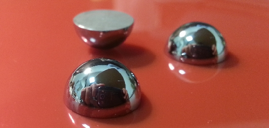
Silicon optical lenses are ideal for collimation or focusing applications that utilize monochromatic light. These lenses are available in a range of sizes or focal lengths for a wide variety of application needs. We also produce HRFZ Si lenses of different types: hyper-/hemispherical for Thz applications
Alkor Technologies produces a wide variety of Silicon Optical Components, including Silicon optical lenses, IR filters, or windows.
Germaniumwindow
This surface roughness indication method pictorially displays information such as the surface roughness value, cutoff value, sampling length, machining method, crease direction symbol, and surface waviness on the surface indication symbol as shown below.
The creases made by the edged tool during machining are at an angle and cross each other on the surface captured in the diagram in which the symbol is written.
Symbols that indicate the surface texture of machined and structural parts are used in industrial diagrams. The pictorial representation using these symbols is defined in ISO 1302:2002.
IR intereference filters, which are integrated into IR applications such as FTIR spectroscopy, are used to transmit or block a specific range of IR wavelengths.
The descriptors shown below are used when pictorially representing surface roughness. However, generally speaking, the standard conditions, which are shown in red, are omitted, and the indications shown in blue are included only when necessary.
Silicon is used for windows and lenses in the 2-6�m range, ideal choice for IR LED lenses. The refractive index is near 3.4 throughout the range. Silicon high thermal conductivity and low weight are attractive features in IR or FTIR applications. Silicon is also used as a high reflectivity mirror substrate for lasers and for IR silicon viewports.


 Ms.Cici
 8618319014500