
Light Pipe (discontinued) - lightpipe
cmossensor vs full-frame
Figure 3: The three main shutter formats. Most CCD/EMCCs have a true global shutter with readout from allpixels simultaneously as they are exposed to light. Most sCMOS sensors have a rolling shutter, whichalthough is fast and has high sensitivity (from back-illuminated sensors) can provide artifacts. Pseudo-global shutters use a trigger to control the light source allowing for a global shutter within the rolling shutter iftimes precisely.
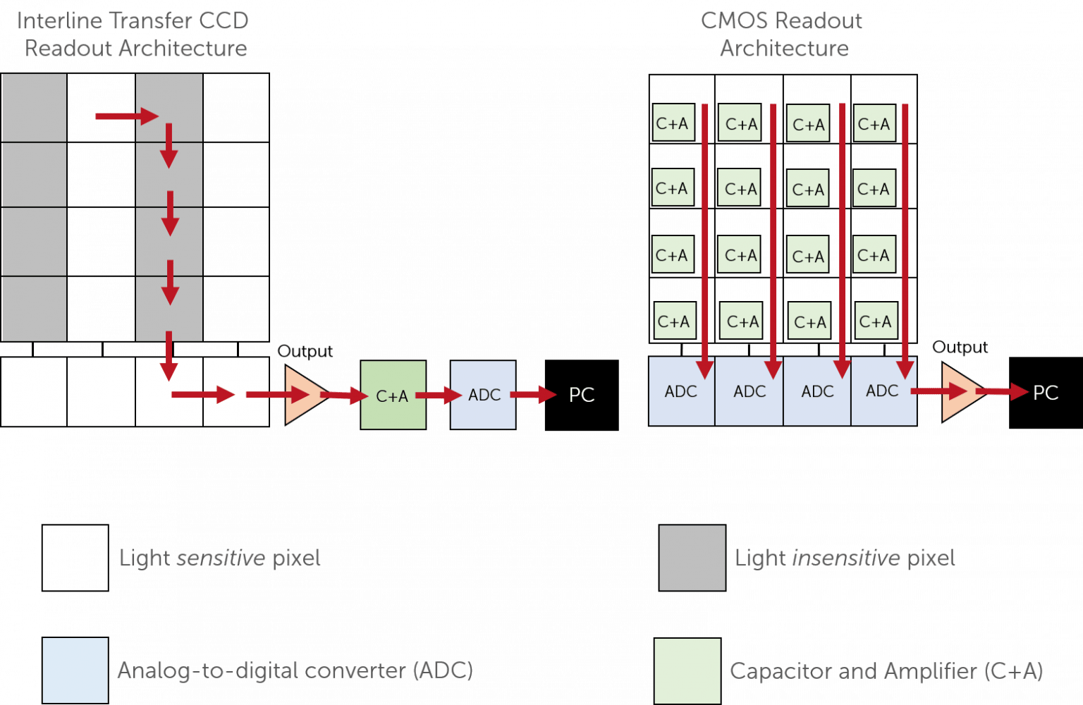
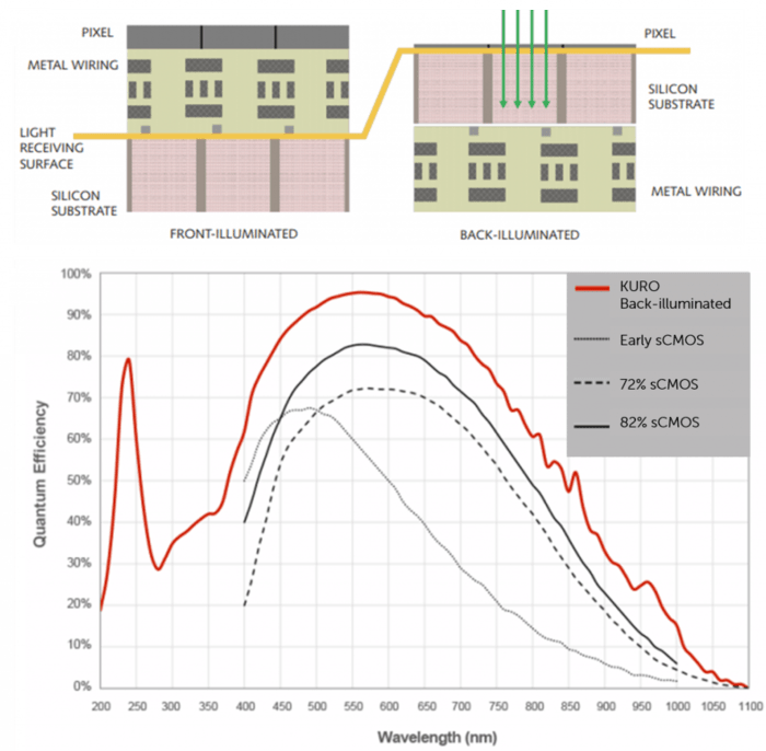
Figure 4: Front vs back-illuminated sCMOS technology. Top: Front-illuminated sensor(left) have lower QE as light is scattered within the pixel and sensor wiring before hittingthe silicon substrate. In back-illuminated sensors (right) the light directly hits the sensor,resulting in a much higher QE. Bottom: QE curve for various front-illuminated sCMOStechnologies (early, 72% and 82% sCMOS) compared with back-illuminated sCMOS technology (peaks at 95% QE with the KURO).
CMOS Cameraprice
Figure 2: Schematic indicating how acquisition of a frame can overlap with the readout of the previous frame. This allows the sCMOS to acquire and readout at a fast speed.
sCMOS sensors take advantage of active circuit integration into individual pixels. This allows each pixel to be read out individually. There is also an analog-to-digital converter attached to each column, allowing much higher frame rates while still maintaining low read noise, large field of view and high power efficiency.
CMOS sensor technology differs from CCD sensors as instead of having all sensor pixels fed through one output node, one amplifier and one analog-to-digital converter (ADC) as with a CCD sensor, CMOS sensors work in parallel by having a miniaturized capacitor and amplifier on every pixel, and an ADC for every column (as shown in Figure 1). Each ADC acts simultaneously, reading out entire columns rather than individual pixels of the whole sensor. This makes the process much faster and requires 100x less power than CCD sensor architecture.
CMOSimage sensor
Rolling shutters switch "on" and "off" by clearing the charge that is already within one row and measuring any new incident photons. This allows for an overlap between the acquisition of the current pixel row of a frame (which is acquiring an image), and the lower pixel rows of the previous frame (of an image being readout) (Figure 2).
Some early sCMOS sensors had issues with background quality and noise, limiting the use of CMOS for more demanding applications. To overcome this, higher sensitivity was required to improve the technology. In 2016, back-illuminated sCMOS was created, offering a peak quantum efficiency (QE) of 95% without compromising pixel size, while also improvements were made to background quality. Figure 4 shows a diagram of back-illuminated sCMOS technology, alongside a QE curve indicating the difference between early sCMOS and back-illuminated sCMOS.
Cmos on cameraiphone
sCMOS sensors differ from CCD sensors as they typically have a rolling shutter. Image acquisition begins at the top of the sensor and works its way down, row by row. This allows the sensor to acquire images at much higher framerates with much lower read noise. The speed of an sCMOS camera directly relates to the number of rows, and the row time (i.e. the time between acquisition of one row and another).
Figure 1: Readout architectures comparing interline transfer CCD and sCMOS sensor. Left: Interline transfer CCD format,in which electrons are shifted off the sensor onto a readout register, output node, amplified (by a capacity (C) and anamplifier (A)) and converted into digital grey levels by an ADC. This is then sent to the computer. Right: Typical CMOSformat, where every pixel has a capacitor and amplifier associated. This means that photons that hit each pixel produceelectrons, which are converted to readable voltage on the pixel. Voltages from the whole column are sent to an ADC (in which there is one per column), and these are sent straight to the computer. This makes CMOS cameras much faster as they work in parallel.
CMOSimage sensor working principle
CMOSsensor
Some sCMOS sensors can be used in a pseudo-global shutter mode for zero distortion and applications involving hardware changes between frames, such as sequential dual-channel acquisition. This pseudo-global shutter takes advantage of controlling the triggering of the light source. To create this global shutter the camera needs to activate the rolling shutter in dark conditions. Then by triggering the light source and stopping the light at the same time as stopping the camera an area of the array can be illuminated simultaneously, just as a global shutter (as shown in Figure 3).
In 2009, scientific CMOS (sCMOS) technology was launched, with sCMOS cameras being commercially available in 2010-11. sCMOS cameras are able to provide low noise, high speed, and a large field of view, making sCMOS cameras ideal for a wide range of applications, from astronomy to microscopy.
The differences in CCD and sCMOS sensor architecture provide both advantages and disadvantages. Some of the advantages of sCMOS technology over CCD technology are as follows:
Complementary metal-oxide-semiconductor (CMOS) sensors are a technology that has been around since the 1990s. Early CMOS cameras were competing with the more mature CCD technology, but over the 1990s and early 2000s CMOS sensor technology improved to the point where CCD technology was overtaken to become the sensor of choice for consumer digital cameras. This technology was then improved further still to fulfil the higher requirements essential for scientific imaging.

Although there is an increase in temporal noise and fixed-pattern noise due to the increase in active circuits on the sensor, sCMOS technology is still advantageous from a wide range of applications.


 Ms.Cici
 8618319014500