
Introduction to Microscopes and Objective Lenses - what is the function of the objectives on a microscope
An objective measure of sharpness which takes into account the sensitivity of the human visual system to specific spatial frequencies and the viewing distance of an image. Edge acutance refers to the ability of a photographic system to show a sharp edge between contiguous areas of low and high illuminance. Texture acutance refers to the ability of a photographic system to show details without noticeable degradations.
For visible and NIR wavelengths, the Silicon (Si) molecule is a good detecting material. Depending on the detector structure Si can convert over 90% of photons into electrons, a measure known as Quantum Efficiency (QE). However, as the wavelengths lengthen past 900 nm (0.9 µm), the efficiency in capturing photons becomes weaker and photons start passing through Si so QE falls, and goes below 1 % past 1100 nm, even with processing tricks used to extend sensitivity.
Optics is an interdisciplinary program that allows students with a variety of backgrounds to explore optics through a variety of lenses.
Due to diffraction of light, conventional microscopy has a practical resolution limit of ∼ λ / ( 2 N A ) , called the Abbe diffraction limit, where λ is the ...
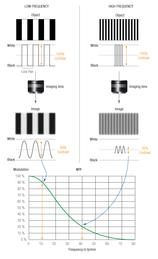
Sharpness is based on the MTF measurement. Let’s start with a practical measurement experiment to help describe what MTF is. If we look at a series of black and white stripes with varying spatial frequency and fixed contrast (same reflectance ratio between black and white, independent of the spatial frequency), we can see that the image of high-frequency stripes has a lower contrast than that for low-frequency stripes. For very high frequencies, the image eventually becomes (almost) uniform, with an intermediate level between black and white, which our eyes perceive as a shade of gray.
Swirmwir lwir
What is the SWIR wavelength region? The shortwave infrared (SWIR) has various definitions, depending on the author. Like most definitions, the meaning of the label has also evolved over time. SWIR is a sub-region of the electromagnetic wavelength spectrum that scientists historically have called the Infrared and is included in the region that spectroscopists referred to as the Near Infrared (NIR). As detector technology developed, the NIR region was bounded by where the human eye can no longer see and where silicon detectors become transparent and lose sensitivity, which is slightly longer than 1 micron (1 µm) in wavelength. For the purposes of this website, which is provided by Princeton Infrared Technologies (PIRT) a SWIR imaging detector company, the SWIR region runs from 1000 to 2600 nm (1.0 to 2.6 µm). This is bounded on the shorter wavelength end by the NIR region from 750 to 1000 nm (0.75 to 1 µm) and on the longer side by the dominant atmospheric absorbance band from 2600 to 3000 nm (2.6 to 3.0 µm). This longer wavelength SWIR boundary is further re-enforced by the end of the transmission window for glass and quartz optics, which is around 2.6 µm.
The resolution of a camera is defined by the size of the smallest detail that the camera can optically discriminate. ISO standard 12233 defines the limiting resolution as the first frequency such that the contrast attenuation is 95% (hence a MTF value of 5%). In practice, this value is very small and is also sensitive to measurement noise
DSLR lenses usually have a radial symmetry, which means that field dependency can be summarized by the MTF at different distances to the image center.
MWIR
by K Kaur · 2023 · Cited by 2 — A prism is a triangular refracting surface with an apex and a base. The incident light ray passing through the prism is refracted so that it is bent towards the ...
Sharpness is a subjective quality attribute of an image or a lens. Sharpness indicates the visually perceived quality of details of an image or details reproduced by a lens. It is associated with both resolution and contrast of reproduced details (within an image or by a lens).
May 11, 2023 — How are DOEs used in coherent beam combining? Diffractive beam splitters are used in CBC to split a single input beam into multiple output beams ...
swir是什么
We plot the acutance as a function of the radial field position, taking into consideration horizontal and vertical directions. We make measurements for several focal lengths and aperture values.
NIRSWIR
Acrylic (PMMA). Acrylic, often known as Plexiglass, is a clear thermoplastic with excellent strength and stiffness and glass-like properties. Acrylic ages well ...
Infrared spectrum
RESOLUTION PATTERN. USAF 1951 TARGET. REFLECTIVE. The target has a high contrast and contains the USAF 1951 groups -2 tho 7. The pattern is repeated twelve.
For the NIR-SWIR range there are various materials that have been tried for imaging. Commercial production currently uses these molecules for detection: InGaAs, NIR extended Si, Ge, Si-Ge, PbSe colloidal quantum dots (CQD), InGaAs/GaAsSb Type 2 Superlattices, InSb, or HgCdTe. In general, for the 1000 to 1680 nm (1.0 to 1.68 µm) range, the material known as lattice matched InGaAs (which is really In.53Ga.47As) offer the best combination of high QE, dynamic range, and image quality with low Size, Weight and Power. When imaging applications need to cover 1000 to 2100 nm (1.0 to 2.1 µm), new solutions based on Type II superlattice structures that have layers of InGaAs alternating with GaAsSb are now available that provide the best QE and image quality of commercially available cameras. In the future one will see Type 2 Strained Layer Superlattices which are more complicated combinations of InGaAs/GaAsSb and these will allow detection to 2600nm. Several alternative products claim to reduce cost compared to InGaAs designs which manually hybridize the photodiode layer to the Read-Out Integrated Circuit (ROIC) for each Focal Plane Array (FPA). However, PIRT uses wafer-scale bonding to substantially reduce the assembly costs, while the so-called low-cost competitors have discovered they still need costly thin-film processing to achieve reliable, and consistent imaging performance.
Get Binoculars &Telescopes from Target to save money and time. Select Same Day Delivery or Drive Up for easy contactless purchases.
DXOMARK encourages its readers to share comments on the articles. To read or post comments, Disqus cookies are required. Change your Cookies Preferences and read more about our Comment Policy.
How are the SWIR wavelengths imaged? Imaging detectors have an absorbance layer that receives light photons and absorb their energies. To be a good detector they must be able to convert the energies into an electrical current, rather than into heat or even reflecting the photons away. In materials that do this conversion well the absorbance layer is typically a semiconductor crystal whose bandgap energy is less than the energy carried by the photon's wavelength.
Laser spectroscopy has led to advances in the precision with which spectral line frequencies can be measured, and this has fundamental significance for our ...
SonySWIR
Because of field aberrations (such as field curvature), the value of the limiting resolution and acutance depends on the field position.

The value of the MTF at frequency 0 is always 100% since a flat field is considered to have been reproduced perfectly, with no intensity loss. Attenuation due to lens transmission is measured separately.
As a leading provider of cutting-edge digital printing solutions, we are dedicated to transforming your ideas into captivating visual masterpieces. Our state-of ...
SWIRcamera
Why are the SWIR, NIR-SWIR and Vis-SWIR bands valuable? The SWIR wavelength range is important because, chemical signatures due to chemical absorption are imprinted on reflected or transmitted light. The images are easier for operators to understand because viewing NIR and SWIR images are like viewing visible light images. There is also reduced scattering in the SWIR band allowing for sharper images while looking through the atmosphere at objects far away. For special cases, the SWIR band has value for thermal imaging as well, such as when object temperatures are >100°C, or need to be viewed through glass or quartz optics or windows.
LWIR
For the DxOMark sharpness score, we compute MTF in horizontal and vertical directions by examining the spatial response of the camera to a perfect edge. This measurement follows ISO standard 12233.
Comments Section ... Assuming you don't need to worry about things overlapping the shifts, potentially just call them shifts A, B and C (or E(arly) ...
The MTF precisely describes the contrast attenuation: for each spatial frequency, the MTF plots the ratio of the output modulation versus the test object modulation.
We map the acutance on a color scale as a function of focal length and aperture value. We make measurements for several field positions.
The DxOMark score for Sharpness is based on the Perceptual Megapixel (P-Mpix) concept that weights the Modulation Transfer Function (MTF) of the lens with the human visual acuity. Read more about Perceptual Megapixels.
As detector technology has developed, there are now low noise Vis-SWIR InGaAs imaging detectors that cover the visible to the middle of the SWIR range, 400 to 1700 nm (0.4 to 1.7 µm), such as the PIRT MVCam, and 1280SciCam. In the past, to extend beyond 1700 nm required changing the InGaAs crystal, this introduced excess dark current and image non-uniformities that made such imaging detectors unattractive to the market, causing some to commercialize low quantum-efficiency (QE) technologies such as colloidal quantum dots (CQD). This is now changing. PIRT has just introduced, a megapixel camera that responds from 400 to 2050 nm (0.4 to 2.05 µm) utilizing a completely different detector structure, one using InGaAs/GaAsSb type-II super lattice (T2SL) technology. This is yielding superior image quality with QE response of >30% at 1550 nm and >20% at 1900 nm (at 1.55 and 1.9 µm) with no imaging artifacts.


 Ms.Cici
 8618319014500