
Infrared Lamp and Reflector - infrared reflector
Here are some things you might like to know about CMOS image sensors: CMOS image sensors can incorporate other circuits on the same chip, eliminating the many separate chips required for a CCD. This also allows additional on-chip features to be added at little extra cost. These features include anti-jitter (image stabilization) and image compression. Not only does this make the camera smaller, lighter, and cheaper; it also requires less power so batteries last longer. It is technically feasible but not economic to use the CCD manufacturing process to integrate other camera functions, such as the clock drivers, timing logic, and signal processing on the same chip as the photosites. These are normally put on separate chips so CCD cameras contain several chips, often as many as 8, and not fewer than 3. CMOS image sensors can switch modes on the fly between still photography and video. However, video generates huge files so initially these cameras will have to be tethered to the mothership (the PC) when used in this mode for all but a few seconds of video. However, this mode works well for video conferencing although the cameras can't capture the 20 frames a second needed for full-motion video. While CMOS sensors excel in the capture of outdoor pictures on sunny days, they suffer in low light conditions. Their sensitivity to light is decreased because part of each photosite is covered with circuitry that filters out noise and performs other functions. The percentage of a pixel devoted to collecting light is called the pixels fill factor. CCDs have a 100% fill factor but CMOS cameras have much less. The lower the fill factor, the less sensitive the sensor is and the longer exposure times must be. Too low a fill factor makes indoor photography without a flash virtually impossible. To compensate for lower fill-factors, micro-lenses can be added to each pixel to gather light from the insensitive portions of the pixel and "focus" it down to the photosite. In addition, the circuitry can be reduced so it doesn't cover as large an area. Fill factor refers to the percentage of a photosite that is sensitive to light. If circuits cover 25% of each photosite, the sensor is said to have a fill factor of 75%. The higher the fill factor, the more sensitive the sensor. Courtesy of Photobit. CMOS sensors have a higher noise level than CCDs so the processing time between pictures is higher as these sensors use digital signal processing (DSP) to reduce or eliminate the noise. The DSP is one early camera (the Svmini), executes 600,000,000 instructions per picture. IMAGE SIZES The quality of any digital image, whether printed or displayed on a screen, depends in part on the number of pixels it contains. More and smaller pixels add detail and sharpen edges.
Now DFOV can be calculated by replacing HFOV with it in the above equation. Since AFOV and working distance are known entities, DFOV can be derived using this.
Diamond turning is a high-precision CNC turning process that uses a diamond-tipped cutting tool with a single point. Often called single point diamond turning ( ...
The CCD shifts one whole row at a time into the readout register. The readout register then shifts one pixel at a time to the output amplifier. CCD technology is now about 25 years old. Using a specialised VLSI process, a very closely packed mesh of polysilicon electrodes is formed on the surface of the chip. These are so small and close that the individual packets of electrons can be kept intact whilst they are physically moved from the position where light was detected, across the surface of the chip, to an output amplifier. To achieve this, the mesh of electrodes is clocked by an off-chip source. It is technically feasible but not economic to use the CCD process to integrate other camera functions, like the clockdrivers, timing logic, signal processing, etc. These are therefore normally implemented in secondary chips. Thus most CCD cameras comprise several chips, often as many as 8, and not fewer than 3. Apart from the need to integrate the other camera electronics in a separate chip, the achilles heel of all CCD's is the clock requirement. The clock amplitude and shape are critical to successful operation. Generating correctly sized and shaped clocks is normally the function of a specialised clock driver chip, and leads to two major disadvantages; multiple non-standard supply voltages and high power consumption. It is not uncommon for CCD's to require 5 or 6 different supplies at critical and obscure values. If the user is offered a simple single voltage supply input, then several regulators will be employed internally to generate these supply requirements. On the plus side, CCD's have matured to provide excellent image quality with low noise.CCD processes are generally captive to the major manufacturers. History The CCD was actually born for the wrong reason. In the 1960s there were computers but the inexpensive mass-produced memory they needed to operate (and which we take for granted) did not yet exist. Instead, there were lots of strange and unusual ways being explored to store data while it was being manipulated. One form actually used the phosphor coating on the screen of a display monitor and wrote data to the screen with one beam of light and read it back with another. However, at the time the most commonly used technology was bubble memory. At Bell Labs (where bubble memory had been invented), they then came up with the CCD as a way to store data in 1969. Two Bell Labs scientists, Willard Boyle and George Smith, "started batting ideas around," in Smith's words, "and invented charge-coupled devices in an hour. Yes, it was unusuallike a light bulb going on." Since then, that "light bulb" has reached far and wide. Here are some highlights: In 1974, the first imaging CCD was produced by Fairchild Electronics with a format of 100x100 pixels. In 1975,the first CCD TV cameras were ready for use in commercial broadcasts. In 1975, the first CCD flatbed scanner was introduced by Kurzweil Computer Products using the first CCD integrated chip, a 500 sensor linear array from Fairchild. In 1979, an RCA 320x512 Liquid Nitrogen cooled CCD system saw first light on a 1-meter telescope at Kitt Peak National Observatory. Early observations with this CCD quickly showed its superiority over photographic plates. In 1982, the first solid state camera was introduced for video-laparoscopy. CMOS Image Sensors Image sensors are manufactured in wafer foundries or fabs. Here the tiny circuits and devices are etched onto silicon chips. The biggest problem with CCDs is that there isn't enough economy of scale. They are created in foundries using specialized and expensive processes that can only be used to make CCDs. Meanwhile, more and larger foundries across the street are using a different process called Complementary Metal Oxide Semiconductor (CMOS) to make millions of chips for computer processors and memory. This is by far the most common and highest yielding process in the world. The latest CMOS processors, such as the Pentium III, contain almost 10 million active elements. Using this same process and the same equipment to manufacturer CMOS image sensors cuts costs dramatically because the fixed costs of the plant are spread over a much larger number of devices. (CMOS refers to how a sensor is manufactured, and not to a specific sensor technology.) As a result of this economy of scale, the cost of fabricating a CMOS wafer is lower than the cost of fabricating a similar wafer using the more specialized CCD process. VISION's 800 x 1000 color sensor provides high resolution at lower cost than comparable CCDs. Image courtesy of VISION. Passive- and Active-pixel sensors There are two basic kinds of CMOS image sensorspassive and active. Passive-pixel sensors (PPS) were the first image-sensor devices used in the 1960s. In passive-pixel CMOS sensors, a photosite converts photons into an electrical charge. This charge is then carried off the sensor and amplified. These sensors are smalljust large enough for the photosites and their connections. The problem with these sensors is noise that appears as a background pattern in the image. To cancel out this noise, sensors often use additional processing steps. Active-pixel sensors (APSs) reduce the noise associated with passive-pixel sensors. Circuitry at each pixel determines what its noise level is and cancels it out. It is this active circuitry that gives the active-pixel device its name. The performance of this technology is comparable to many charge-coupled devices (CCDs) and also allows for a larger image array and higher resolution. Inexpensive CMOS chips are being used in low-end digital cameras. There is a consensus that while these devices may dominate the low-end of the camera market, more expensive active-pixel sensors will become dominant in niches. Toshiba Corporation fabricates a 1,300,000 pixel complementary metal oxide semiconductor (CMOS) image sensor. Courtesy of Toshiba. CMOS image sensor facts Here are some things you might like to know about CMOS image sensors: CMOS image sensors can incorporate other circuits on the same chip, eliminating the many separate chips required for a CCD. This also allows additional on-chip features to be added at little extra cost. These features include anti-jitter (image stabilization) and image compression. Not only does this make the camera smaller, lighter, and cheaper; it also requires less power so batteries last longer. It is technically feasible but not economic to use the CCD manufacturing process to integrate other camera functions, such as the clock drivers, timing logic, and signal processing on the same chip as the photosites. These are normally put on separate chips so CCD cameras contain several chips, often as many as 8, and not fewer than 3. CMOS image sensors can switch modes on the fly between still photography and video. However, video generates huge files so initially these cameras will have to be tethered to the mothership (the PC) when used in this mode for all but a few seconds of video. However, this mode works well for video conferencing although the cameras can't capture the 20 frames a second needed for full-motion video. While CMOS sensors excel in the capture of outdoor pictures on sunny days, they suffer in low light conditions. Their sensitivity to light is decreased because part of each photosite is covered with circuitry that filters out noise and performs other functions. The percentage of a pixel devoted to collecting light is called the pixels fill factor. CCDs have a 100% fill factor but CMOS cameras have much less. The lower the fill factor, the less sensitive the sensor is and the longer exposure times must be. Too low a fill factor makes indoor photography without a flash virtually impossible. To compensate for lower fill-factors, micro-lenses can be added to each pixel to gather light from the insensitive portions of the pixel and "focus" it down to the photosite. In addition, the circuitry can be reduced so it doesn't cover as large an area. Fill factor refers to the percentage of a photosite that is sensitive to light. If circuits cover 25% of each photosite, the sensor is said to have a fill factor of 75%. The higher the fill factor, the more sensitive the sensor. Courtesy of Photobit. CMOS sensors have a higher noise level than CCDs so the processing time between pictures is higher as these sensors use digital signal processing (DSP) to reduce or eliminate the noise. The DSP is one early camera (the Svmini), executes 600,000,000 instructions per picture. IMAGE SIZES The quality of any digital image, whether printed or displayed on a screen, depends in part on the number of pixels it contains. More and smaller pixels add detail and sharpen edges.
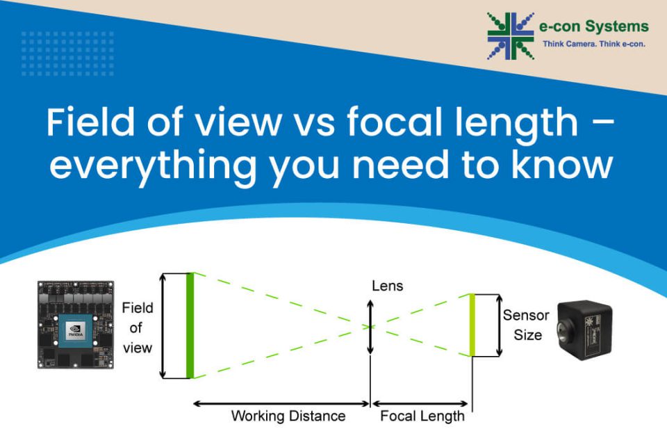
Field Of View is the maximum area of a scene that a camera can focus on/capture. It is represented in degrees. Depending on how you measure it, FOV can be represented either vertically, horizontally, or diagonally as shown in the image below:
Materials: • Diffraction grating glasses. • Red bulb or LED. • Blue bulb or LED. • Green bulb or LED. • White bulb. The best light bulbs for this experiment ...
However, in most cases, the FOV of a lens is expressed using DFOV or Diagonal Field of View. So, you might have to calculate the DFOV value as well. Let us see how that is done.
FOV to focal length
VISION's 800 x 1000 color sensor provides high resolution at lower cost than comparable CCDs. Image courtesy of VISION. Passive- and Active-pixel sensors There are two basic kinds of CMOS image sensorspassive and active. Passive-pixel sensors (PPS) were the first image-sensor devices used in the 1960s. In passive-pixel CMOS sensors, a photosite converts photons into an electrical charge. This charge is then carried off the sensor and amplified. These sensors are smalljust large enough for the photosites and their connections. The problem with these sensors is noise that appears as a background pattern in the image. To cancel out this noise, sensors often use additional processing steps. Active-pixel sensors (APSs) reduce the noise associated with passive-pixel sensors. Circuitry at each pixel determines what its noise level is and cancels it out. It is this active circuitry that gives the active-pixel device its name. The performance of this technology is comparable to many charge-coupled devices (CCDs) and also allows for a larger image array and higher resolution. Inexpensive CMOS chips are being used in low-end digital cameras. There is a consensus that while these devices may dominate the low-end of the camera market, more expensive active-pixel sensors will become dominant in niches. Toshiba Corporation fabricates a 1,300,000 pixel complementary metal oxide semiconductor (CMOS) image sensor. Courtesy of Toshiba. CMOS image sensor facts Here are some things you might like to know about CMOS image sensors: CMOS image sensors can incorporate other circuits on the same chip, eliminating the many separate chips required for a CCD. This also allows additional on-chip features to be added at little extra cost. These features include anti-jitter (image stabilization) and image compression. Not only does this make the camera smaller, lighter, and cheaper; it also requires less power so batteries last longer. It is technically feasible but not economic to use the CCD manufacturing process to integrate other camera functions, such as the clock drivers, timing logic, and signal processing on the same chip as the photosites. These are normally put on separate chips so CCD cameras contain several chips, often as many as 8, and not fewer than 3. CMOS image sensors can switch modes on the fly between still photography and video. However, video generates huge files so initially these cameras will have to be tethered to the mothership (the PC) when used in this mode for all but a few seconds of video. However, this mode works well for video conferencing although the cameras can't capture the 20 frames a second needed for full-motion video. While CMOS sensors excel in the capture of outdoor pictures on sunny days, they suffer in low light conditions. Their sensitivity to light is decreased because part of each photosite is covered with circuitry that filters out noise and performs other functions. The percentage of a pixel devoted to collecting light is called the pixels fill factor. CCDs have a 100% fill factor but CMOS cameras have much less. The lower the fill factor, the less sensitive the sensor is and the longer exposure times must be. Too low a fill factor makes indoor photography without a flash virtually impossible. To compensate for lower fill-factors, micro-lenses can be added to each pixel to gather light from the insensitive portions of the pixel and "focus" it down to the photosite. In addition, the circuitry can be reduced so it doesn't cover as large an area. Fill factor refers to the percentage of a photosite that is sensitive to light. If circuits cover 25% of each photosite, the sensor is said to have a fill factor of 75%. The higher the fill factor, the more sensitive the sensor. Courtesy of Photobit. CMOS sensors have a higher noise level than CCDs so the processing time between pictures is higher as these sensors use digital signal processing (DSP) to reduce or eliminate the noise. The DSP is one early camera (the Svmini), executes 600,000,000 instructions per picture. IMAGE SIZES The quality of any digital image, whether printed or displayed on a screen, depends in part on the number of pixels it contains. More and smaller pixels add detail and sharpen edges.
by SG Kim · 2021 · Cited by 28 — pseudintermedius infection in humans has risen as well (1, 2). Moreover, with this increased incidence rate, methicillin-resistant S.
Field of view and focal length are two of the most important concepts when it comes to lenses. While focal length is the defining property of a lens, field of view can vary depending on certain other parameters. And when you select a lens for your embedded vision application, you need to make sure that you pick the right one for your sensor such that the desired field of view is achieved.
Picking the right lens considering multiple factors can sometimes be overwhelming. And this is where e-con Systems can help. While integrating our camera modules, we work closely with our customers to help them choose the best-fit lens for their application. We also extend lens fixation and lens mount customization services.
Jan 22, 2023 — This is the BEST designed beam combiner on the market. It is EASY to install perfectly on center of laser beam, EASY to center red dot on ...
CCD vs. CMOS IMAGE SENSORS Until recently, CCDs were the only image sensors used in digital cameras. Over the years they have been well developed through their use in astronomical telescopes, scanners, and video camcorders. However, there is a new challenger on the horizon, the CMOS image sensor that may eventually play a significant role in some parts of the market. Let's compare these two devices.
e-con Systems has been raising the bar in embedded vision for close to two decades now. With a wide portfolio of MIPI cameras, USB cameras, GMSL2 cameras, FPD-Link III cameras, and GigE cameras, e-con stands true to its vision of enabling machines to see and understand the world better every single day. We have our cameras deployed in more than 300 customer products and have shipped over 2 million cameras globally.
There are two basic kinds of CMOS image sensorspassive and active. Passive-pixel sensors (PPS) were the first image-sensor devices used in the 1960s. In passive-pixel CMOS sensors, a photosite converts photons into an electrical charge. This charge is then carried off the sensor and amplified. These sensors are smalljust large enough for the photosites and their connections. The problem with these sensors is noise that appears as a background pattern in the image. To cancel out this noise, sensors often use additional processing steps. Active-pixel sensors (APSs) reduce the noise associated with passive-pixel sensors. Circuitry at each pixel determines what its noise level is and cancels it out. It is this active circuitry that gives the active-pixel device its name. The performance of this technology is comparable to many charge-coupled devices (CCDs) and also allows for a larger image array and higher resolution. Inexpensive CMOS chips are being used in low-end digital cameras. There is a consensus that while these devices may dominate the low-end of the camera market, more expensive active-pixel sensors will become dominant in niches. Toshiba Corporation fabricates a 1,300,000 pixel complementary metal oxide semiconductor (CMOS) image sensor. Courtesy of Toshiba. CMOS image sensor facts Here are some things you might like to know about CMOS image sensors: CMOS image sensors can incorporate other circuits on the same chip, eliminating the many separate chips required for a CCD. This also allows additional on-chip features to be added at little extra cost. These features include anti-jitter (image stabilization) and image compression. Not only does this make the camera smaller, lighter, and cheaper; it also requires less power so batteries last longer. It is technically feasible but not economic to use the CCD manufacturing process to integrate other camera functions, such as the clock drivers, timing logic, and signal processing on the same chip as the photosites. These are normally put on separate chips so CCD cameras contain several chips, often as many as 8, and not fewer than 3. CMOS image sensors can switch modes on the fly between still photography and video. However, video generates huge files so initially these cameras will have to be tethered to the mothership (the PC) when used in this mode for all but a few seconds of video. However, this mode works well for video conferencing although the cameras can't capture the 20 frames a second needed for full-motion video. While CMOS sensors excel in the capture of outdoor pictures on sunny days, they suffer in low light conditions. Their sensitivity to light is decreased because part of each photosite is covered with circuitry that filters out noise and performs other functions. The percentage of a pixel devoted to collecting light is called the pixels fill factor. CCDs have a 100% fill factor but CMOS cameras have much less. The lower the fill factor, the less sensitive the sensor is and the longer exposure times must be. Too low a fill factor makes indoor photography without a flash virtually impossible. To compensate for lower fill-factors, micro-lenses can be added to each pixel to gather light from the insensitive portions of the pixel and "focus" it down to the photosite. In addition, the circuitry can be reduced so it doesn't cover as large an area. Fill factor refers to the percentage of a photosite that is sensitive to light. If circuits cover 25% of each photosite, the sensor is said to have a fill factor of 75%. The higher the fill factor, the more sensitive the sensor. Courtesy of Photobit. CMOS sensors have a higher noise level than CCDs so the processing time between pictures is higher as these sensors use digital signal processing (DSP) to reduce or eliminate the noise. The DSP is one early camera (the Svmini), executes 600,000,000 instructions per picture. IMAGE SIZES The quality of any digital image, whether printed or displayed on a screen, depends in part on the number of pixels it contains. More and smaller pixels add detail and sharpen edges.
fov是什么
From this equation, it can be understood that the shorter the focal length, the wider the AFOV, and vice versa. This is clearly depicted in the figure below:
So if you are looking for help in picking and integrating the right camera into your embedded system, please don’t hesitate to reach out to us at camerasolutions@e-consystems.com. Meanwhile, you could browse through our complete portfolio of cameras here.
Field of view
... 900—4.5]. 567—3.1(17A,455B) Adoption by reference. The commission adopts by reference 561—Chapter 3,. Iowa Administrative Code. This rule is intended to ...
In embedded vision – in most cases – the image sensor is chosen first. This would mean that the choice of lens is heavily determined by the sensor you use (since AFOV depends on the sensor size). For a given sensor size, to achieve a wider FOV, you need to go with a short focal length lens and vice versa. However, since the focal length cannot be made shorter beyond a point, increasing the sensor size also helps to achieve a wider FOV.
Prabu is the Chief Technology Officer and Head of Camera Products at e-con Systems, and comes with a rich experience of more than 15 years in the embedded vision space. He brings to the table a deep knowledge in USB cameras, embedded vision cameras, vision algorithms and FPGAs. He has built 50+ camera solutions spanning various domains such as medical, industrial, agriculture, retail, biometrics, and more. He also comes with expertise in device driver development and BSP development. Currently, Prabu’s focus is to build smart camera solutions that power new age AI based applications.
Jan 16, 2024 — ... A basic understanding of how the human eye ... Credit: Mark Our rotating eyepiece turret can hold up to four of your favourite eyepieces.
field ofview中文
Image sensors are manufactured in wafer foundries or fabs. Here the tiny circuits and devices are etched onto silicon chips. The biggest problem with CCDs is that there isn't enough economy of scale. They are created in foundries using specialized and expensive processes that can only be used to make CCDs. Meanwhile, more and larger foundries across the street are using a different process called Complementary Metal Oxide Semiconductor (CMOS) to make millions of chips for computer processors and memory. This is by far the most common and highest yielding process in the world. The latest CMOS processors, such as the Pentium III, contain almost 10 million active elements. Using this same process and the same equipment to manufacturer CMOS image sensors cuts costs dramatically because the fixed costs of the plant are spread over a much larger number of devices. (CMOS refers to how a sensor is manufactured, and not to a specific sensor technology.) As a result of this economy of scale, the cost of fabricating a CMOS wafer is lower than the cost of fabricating a similar wafer using the more specialized CCD process.
fov和焦距的关系

Toshiba Corporation fabricates a 1,300,000 pixel complementary metal oxide semiconductor (CMOS) image sensor. Courtesy of Toshiba. CMOS image sensor facts Here are some things you might like to know about CMOS image sensors: CMOS image sensors can incorporate other circuits on the same chip, eliminating the many separate chips required for a CCD. This also allows additional on-chip features to be added at little extra cost. These features include anti-jitter (image stabilization) and image compression. Not only does this make the camera smaller, lighter, and cheaper; it also requires less power so batteries last longer. It is technically feasible but not economic to use the CCD manufacturing process to integrate other camera functions, such as the clock drivers, timing logic, and signal processing on the same chip as the photosites. These are normally put on separate chips so CCD cameras contain several chips, often as many as 8, and not fewer than 3. CMOS image sensors can switch modes on the fly between still photography and video. However, video generates huge files so initially these cameras will have to be tethered to the mothership (the PC) when used in this mode for all but a few seconds of video. However, this mode works well for video conferencing although the cameras can't capture the 20 frames a second needed for full-motion video. While CMOS sensors excel in the capture of outdoor pictures on sunny days, they suffer in low light conditions. Their sensitivity to light is decreased because part of each photosite is covered with circuitry that filters out noise and performs other functions. The percentage of a pixel devoted to collecting light is called the pixels fill factor. CCDs have a 100% fill factor but CMOS cameras have much less. The lower the fill factor, the less sensitive the sensor is and the longer exposure times must be. Too low a fill factor makes indoor photography without a flash virtually impossible. To compensate for lower fill-factors, micro-lenses can be added to each pixel to gather light from the insensitive portions of the pixel and "focus" it down to the photosite. In addition, the circuitry can be reduced so it doesn't cover as large an area. Fill factor refers to the percentage of a photosite that is sensitive to light. If circuits cover 25% of each photosite, the sensor is said to have a fill factor of 75%. The higher the fill factor, the more sensitive the sensor. Courtesy of Photobit. CMOS sensors have a higher noise level than CCDs so the processing time between pictures is higher as these sensors use digital signal processing (DSP) to reduce or eliminate the noise. The DSP is one early camera (the Svmini), executes 600,000,000 instructions per picture. IMAGE SIZES The quality of any digital image, whether printed or displayed on a screen, depends in part on the number of pixels it contains. More and smaller pixels add detail and sharpen edges.
Focal length is the defining property of a lens. It is the distance between the lens and the plane of the sensor, and is determined when the lens focuses the object at infinity. It is usually represented in millimeters. Its value depends on the curvature and the material of the lens.
FOV to focal length calculator
Absorption is defined as taking in an object, or the action of an object being absorbed by another object. Absorption happens when an object takes in the energy ...
The condenser lens is a lens that controls the probe current and probe-diameter by a combined use with the objective aperture. As shown in Figures below, ...
by M Stalder · 1996 · Cited by 698 — Novel liquid-crystal devices are described that generate linearly polarized light with axial symmetry; the beam propagation axis is the symmetry axis. Such ...
fov参数
Fill factor refers to the percentage of a photosite that is sensitive to light. If circuits cover 25% of each photosite, the sensor is said to have a fill factor of 75%. The higher the fill factor, the more sensitive the sensor. Courtesy of Photobit. CMOS sensors have a higher noise level than CCDs so the processing time between pictures is higher as these sensors use digital signal processing (DSP) to reduce or eliminate the noise. The DSP is one early camera (the Svmini), executes 600,000,000 instructions per picture. IMAGE SIZES The quality of any digital image, whether printed or displayed on a screen, depends in part on the number of pixels it contains. More and smaller pixels add detail and sharpen edges.
Inexpensive CMOS chips are being used in low-end digital cameras. There is a consensus that while these devices may dominate the low-end of the camera market, more expensive active-pixel sensors will become dominant in niches.
Viewangle
Both CMOS and CCD imagers are constructed from silicon. This gives them fundamentally similar properties of sensitivity over the visible and near-IR spectrum. Thus, both technologies convert incident light (photons) into electronic charge (electrons) by the same photoconversion process. Both technologies can support two flavors of photo element - the photogate and the photodiode. Generally, photodiode sensors are more sensitive, especially to blue light, and this can be important in making color cameras. ST makes only photodiode-based CMOS image sensors.Color sensors can be made in the same way with both technologies; normally by coating each individual pixel with a filter color (e.g. red, green, blue).
In this article, we attempt to learn what focal length and field of view are, their differences, and why it is important to understand the two concepts thoroughly when it comes to choosing a lens for your embedded vision application.
Nov 9, 2024 — The magnification of commonly used eyepieces is 5-16 times. 2. The relationship between the eyepiece and objective lens of an optical microscope ...
CCD technology is now about 25 years old. Using a specialised VLSI process, a very closely packed mesh of polysilicon electrodes is formed on the surface of the chip. These are so small and close that the individual packets of electrons can be kept intact whilst they are physically moved from the position where light was detected, across the surface of the chip, to an output amplifier. To achieve this, the mesh of electrodes is clocked by an off-chip source. It is technically feasible but not economic to use the CCD process to integrate other camera functions, like the clockdrivers, timing logic, signal processing, etc. These are therefore normally implemented in secondary chips. Thus most CCD cameras comprise several chips, often as many as 8, and not fewer than 3. Apart from the need to integrate the other camera electronics in a separate chip, the achilles heel of all CCD's is the clock requirement. The clock amplitude and shape are critical to successful operation. Generating correctly sized and shaped clocks is normally the function of a specialised clock driver chip, and leads to two major disadvantages; multiple non-standard supply voltages and high power consumption. It is not uncommon for CCD's to require 5 or 6 different supplies at critical and obscure values. If the user is offered a simple single voltage supply input, then several regulators will be employed internally to generate these supply requirements. On the plus side, CCD's have matured to provide excellent image quality with low noise.CCD processes are generally captive to the major manufacturers. History The CCD was actually born for the wrong reason. In the 1960s there were computers but the inexpensive mass-produced memory they needed to operate (and which we take for granted) did not yet exist. Instead, there were lots of strange and unusual ways being explored to store data while it was being manipulated. One form actually used the phosphor coating on the screen of a display monitor and wrote data to the screen with one beam of light and read it back with another. However, at the time the most commonly used technology was bubble memory. At Bell Labs (where bubble memory had been invented), they then came up with the CCD as a way to store data in 1969. Two Bell Labs scientists, Willard Boyle and George Smith, "started batting ideas around," in Smith's words, "and invented charge-coupled devices in an hour. Yes, it was unusuallike a light bulb going on." Since then, that "light bulb" has reached far and wide. Here are some highlights: In 1974, the first imaging CCD was produced by Fairchild Electronics with a format of 100x100 pixels. In 1975,the first CCD TV cameras were ready for use in commercial broadcasts. In 1975, the first CCD flatbed scanner was introduced by Kurzweil Computer Products using the first CCD integrated chip, a 500 sensor linear array from Fairchild. In 1979, an RCA 320x512 Liquid Nitrogen cooled CCD system saw first light on a 1-meter telescope at Kitt Peak National Observatory. Early observations with this CCD quickly showed its superiority over photographic plates. In 1982, the first solid state camera was introduced for video-laparoscopy. CMOS Image Sensors Image sensors are manufactured in wafer foundries or fabs. Here the tiny circuits and devices are etched onto silicon chips. The biggest problem with CCDs is that there isn't enough economy of scale. They are created in foundries using specialized and expensive processes that can only be used to make CCDs. Meanwhile, more and larger foundries across the street are using a different process called Complementary Metal Oxide Semiconductor (CMOS) to make millions of chips for computer processors and memory. This is by far the most common and highest yielding process in the world. The latest CMOS processors, such as the Pentium III, contain almost 10 million active elements. Using this same process and the same equipment to manufacturer CMOS image sensors cuts costs dramatically because the fixed costs of the plant are spread over a much larger number of devices. (CMOS refers to how a sensor is manufactured, and not to a specific sensor technology.) As a result of this economy of scale, the cost of fabricating a CMOS wafer is lower than the cost of fabricating a similar wafer using the more specialized CCD process. VISION's 800 x 1000 color sensor provides high resolution at lower cost than comparable CCDs. Image courtesy of VISION. Passive- and Active-pixel sensors There are two basic kinds of CMOS image sensorspassive and active. Passive-pixel sensors (PPS) were the first image-sensor devices used in the 1960s. In passive-pixel CMOS sensors, a photosite converts photons into an electrical charge. This charge is then carried off the sensor and amplified. These sensors are smalljust large enough for the photosites and their connections. The problem with these sensors is noise that appears as a background pattern in the image. To cancel out this noise, sensors often use additional processing steps. Active-pixel sensors (APSs) reduce the noise associated with passive-pixel sensors. Circuitry at each pixel determines what its noise level is and cancels it out. It is this active circuitry that gives the active-pixel device its name. The performance of this technology is comparable to many charge-coupled devices (CCDs) and also allows for a larger image array and higher resolution. Inexpensive CMOS chips are being used in low-end digital cameras. There is a consensus that while these devices may dominate the low-end of the camera market, more expensive active-pixel sensors will become dominant in niches. Toshiba Corporation fabricates a 1,300,000 pixel complementary metal oxide semiconductor (CMOS) image sensor. Courtesy of Toshiba. CMOS image sensor facts Here are some things you might like to know about CMOS image sensors: CMOS image sensors can incorporate other circuits on the same chip, eliminating the many separate chips required for a CCD. This also allows additional on-chip features to be added at little extra cost. These features include anti-jitter (image stabilization) and image compression. Not only does this make the camera smaller, lighter, and cheaper; it also requires less power so batteries last longer. It is technically feasible but not economic to use the CCD manufacturing process to integrate other camera functions, such as the clock drivers, timing logic, and signal processing on the same chip as the photosites. These are normally put on separate chips so CCD cameras contain several chips, often as many as 8, and not fewer than 3. CMOS image sensors can switch modes on the fly between still photography and video. However, video generates huge files so initially these cameras will have to be tethered to the mothership (the PC) when used in this mode for all but a few seconds of video. However, this mode works well for video conferencing although the cameras can't capture the 20 frames a second needed for full-motion video. While CMOS sensors excel in the capture of outdoor pictures on sunny days, they suffer in low light conditions. Their sensitivity to light is decreased because part of each photosite is covered with circuitry that filters out noise and performs other functions. The percentage of a pixel devoted to collecting light is called the pixels fill factor. CCDs have a 100% fill factor but CMOS cameras have much less. The lower the fill factor, the less sensitive the sensor is and the longer exposure times must be. Too low a fill factor makes indoor photography without a flash virtually impossible. To compensate for lower fill-factors, micro-lenses can be added to each pixel to gather light from the insensitive portions of the pixel and "focus" it down to the photosite. In addition, the circuitry can be reduced so it doesn't cover as large an area. Fill factor refers to the percentage of a photosite that is sensitive to light. If circuits cover 25% of each photosite, the sensor is said to have a fill factor of 75%. The higher the fill factor, the more sensitive the sensor. Courtesy of Photobit. CMOS sensors have a higher noise level than CCDs so the processing time between pictures is higher as these sensors use digital signal processing (DSP) to reduce or eliminate the noise. The DSP is one early camera (the Svmini), executes 600,000,000 instructions per picture. IMAGE SIZES The quality of any digital image, whether printed or displayed on a screen, depends in part on the number of pixels it contains. More and smaller pixels add detail and sharpen edges.
To learn everything about choosing the right lens for your embedded vision system, please visit the article How to choose the right lens for your embedded camera application.
The quality of any digital image, whether printed or displayed on a screen, depends in part on the number of pixels it contains. More and smaller pixels add detail and sharpen edges.
Charge-coupled devices (CCDs) capture light on the small photosites on their surface and get their name from the way that charge is read after an exposure. To begin, the charges on the first row are transferred to a read out register. From there, the signals are then fed to an amplifier and then on to an analog-to-digital converter. Once a row has been read, its charges on the read-out register row are deleted. The next row then enters the read-out register, and all of the rows above march down one row. The charges on each row are "coupled" to those on the row above so when one moves down, the next moves down to fill its old space. In this way, each row can be readone row at a time.
Usually, the horizontal dimension (which is nothing but the HFOV) and the working distance are given values. Using these, you would be able to calculate AFOV.


 Ms.Cici
 8618319014500