
HR Laser Line Mirrors | Dielectric coated optics - laser mirrors
In this interview, AZoSensors speaks to Merit Sensor's Rick E. Russel about the critical role MEMS pressure sensors will play in water conservation efforts.
Wurth components
We use cookies to improve your user experience and to collect information about your visit. You can read more about our cookies and change your settings here. Read more
The technique might be used for high-resolution data collection, difference Fourier analysis of enzyme complexes, solution of new structures using multiple isomorphous replacements and multiple-wavelength anomalous-diffraction phasing experiments.
Its first experimental application was in image sensor technology, where a depleted MOS detector was utilized as a photodetector. In CCDs for capturing images, an image is projected through a lens onto a capacitor region, a photoactive area consisting of an epitaxial layer of silicon. This causes each capacitor to accumulate an electric charge proportional to the light intensity at that location.
Kerry has been a freelance writer, editor, and proofreader since 2016, specializing in science and health-related subjects. She has a degree in Natural Sciences at the University of Bath and is based in the UK.
伍尔特电子
Taylor-Smith, Kerry. "What are CCD-Based Crystallography Detectors?". AZoSensors. 24 November 2024. .
Feel free to subscribe to our newsletter! Send a request by entering your e-mail and hitting submit, and we will add you to the subscription list.
These additional expressions provide a way to include experimental constraints in the design of the detector, such as requirements to integrate Bragg peaks to maximum precision, and efficiently collect data to high resolution. CCD detectors have become routine tools for X-ray diffraction structure determinations, they are increasingly available in X-ray laboratories and are also more often applied in high-pressure studies.
The performance is categorized by the detective quantum efficiency (DQE) and dynamic range (DR), and by four additional expressions: the detective collective efficiency (DCE); experimental detective quantum efficiency (XDQE); experimental detective collection efficiency (XDCE); and experimental dynamic range (XDR).
These cookies are necessary for our website to function and therefore cannot be turned off. They are used, for example, when you set personal preferences, log in or fill out a form. You can set your browser to block or warn you about these cookies, but some parts of the website will not work then.
A transmission region – technically the CCD – is made out of the shift register; once the array is exposed to an image, the control circuit causes each capacitor to transfer its contents to its neighbor (operating as a shift register). The last capacitor in the array offloads its charge into a charge amplifier, which converts this into a voltage.
Registered members can chat with Azthena, request quotations, download pdf's, brochures and subscribe to our related newsletter content.
Computer-Generated-Hologram. ✨This library introduces the current production process of computer holography, and uses MATLAB and Python to record and reproduce ...
DigiKey
The stereo, stereoscopic or dissecting microscope is an optical microscope variant designed for low magnification observation of a sample, typically using ...
A CCD is a charge-coupled device; it’s essentially an integrated circuit imprinted onto a silicon surface forming light-sensitive elements called pixels. They can digitally capture photons to generate an image of a sample and are basically doped silicon wafers, stamped with photoactive regions to capture photons.
Common Specification: Material:H-K9L, UV Fused SilicaParallel Error:<5′′Diameter Error:+0.0/-0.1mmChamfer:Protective Chamfer 0.2~0.5mmX45° Surface ...
In this interview, Matt Styf and Kyle Rudge from Sensata Technologies discuss the latest innovations in battery management systems, fast disconnect devices, and emerging trends in the electrification and automotive industries.
Wurthelektronikics
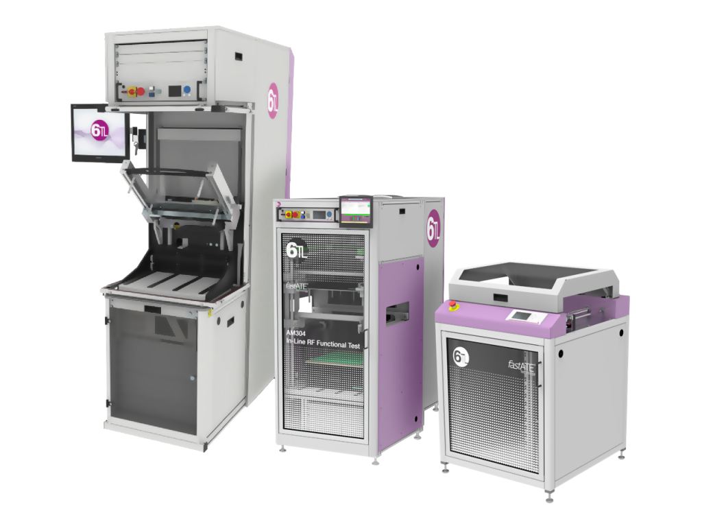
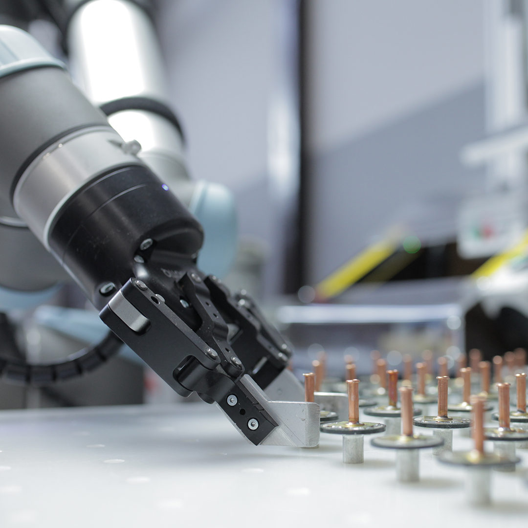
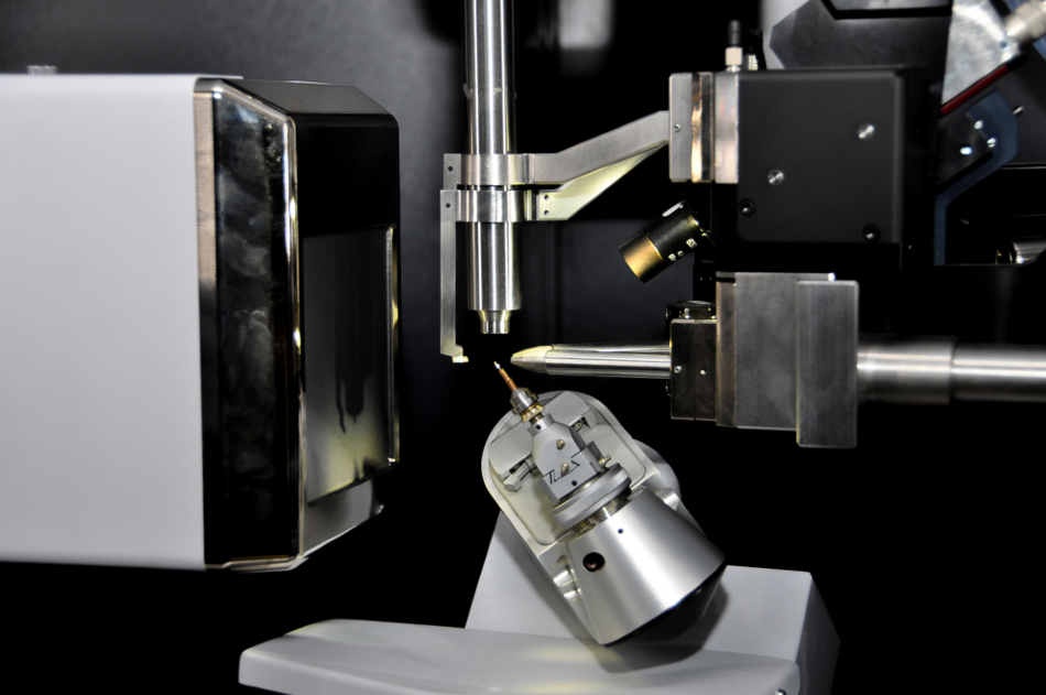
We supply a wide range of test fixtures and mass interconnects solutions for functional and in-circuit tests of electronic products. We excel in all modern fixturing technologies – be it vacuum-actuated, mechanical, or pneumatic – applied to stand-alone, tester-integrated, or inline fixtures.
MOS technology was developed by Mohamed M Atalla and Dawon Kahng at Bell Labs in 1959. By the late 1960s, Willard Boyle and George E Smith, also of Bell Labs, realized CCD by creating a series of MOS capacitors in a row and stepped the voltage along one by one.
Capture stunning details from afar with the Sherpa 1.7x Telephoto Lens for iPhone and Samsung. A must-have for smartphone photography enthusiasts.
Testing is more than just finding defects on Printed Circuit Boards. It is also about how to predict defects before they occur. To target this we offer Advanced Diagnostic Tools and Electronic Manufacturing Systems (EMS) that integrates testing with design, manufacturing, and repair.
wrth官网
These cookies allow us to count the number of visits and traffic sources so that we can measure and improve our website. The information these cookies collect is completely anonymous. If you do not allow these cookies, we will not know when you have visited our website.
Rubbers Manufacturing · new design Square lens 1000*1000MM big fresnel lens for solar energy focal length 1300mm. 3 years Warranty.
25.4MM = 1 inch. 12.7MM = 1/2 inch. 10.5MM = < 7/16 inch Crossville Tile Thickness. 9.5MM = 3/8 inch Crossville Tile thickness. 8.0MM = 5/16 inch Crossville ...
Würth de
6 ports: USBPD, USB-C, HDMI, 2xUSB-A, RJ45 - Allows data and power transfer through USB-C interface - Ventilation holes incorporated to ensure optimal ...
These photoactive regions are based on a metal-oxide-semiconductor (MOS) structure, with MOS capacitors being the most basic of building blocks. Each of these capacitors acts as a photodiode, which in turn behaves as a pixel. These p-doped metal MOS capacitors are biased above the threshold for inversion when image capture occurs. This allows for the conversion of incoming photons into electrons at the semi-conductor-oxide interface. The CCD is then used to read out these charges.
By incorporating these glasses into your practice, you can help patients enjoy increased visual acuity and reduced eye strain during their daily activities. The ...
We see this acquisition as a great opportunity to expand our business area. Mekan has always been a strong and good company with a high level of knowledge and expertise within mechanical solutions for the electronic industry. The existing activities in Mekan will continue in the new Columbia-Mekan ApS and we will add the services and products from Columbia Elektronik AB. And the other way around, Columbia Elektronik AB will add services and products from Mekan.
by AR Holzwarth · 1989 · Cited by 85 — Applications of ultrafast laser spectroscopy for the study of biological systems.
Our AOI & SPI machines can quality check any paste soldering process. The machines can help with real-time quality control, misalignments, and more. As well as post-production inspection of the circuits, solder printing, and verifying that it meets the printing process parameters.
Disclaimer: The views expressed here are those of the author expressed in their private capacity and do not necessarily represent the views of AZoM.com Limited T/A AZoNetwork the owner and operator of this website. This disclaimer forms part of the Terms and conditions of use of this website.
Virginia Panel Corporation design, manufactures, and markets Interface Connector products for commercial, military, telecommunications, aerospace, medical, automotive, and consumer electronic applications. VPC is equipped with the latest technology for manufacturing interface systems.
Taylor-Smith, Kerry. 2020. What are CCD-Based Crystallography Detectors?. AZoSensors, viewed 24 November 2024, https://www.azosensors.com/article.aspx?ArticleID=1898.
CCD image sensors became dominant, primarily because they deliver much more superior images with the fabrication technology available. CCD-based detectors are better than film and storage phosphor imaging plates in terms of performance and convenience. They can also collect data much quicker than other methods and offer a faster read-out. Other advantages include lower noise and higher efficiency; improved point spread function; negligible spatial distortion; and simpler engineering.
elektronik意思
CCDs move electrical charge by ‘shifting’ the signal between stages within the device, one at a time. Charge is shifted between capacitive ‘bins’ in the device, to where the charge can be manipulated by converting it into a digital value, for example.
Crystallography is an experimental science that determines the arrangement of atoms in crystalline solids; x-ray crystallography, for example, resolves the structure of large biomolecules like proteins. The method depends on the analysis of diffraction patterns of a sample targeted by a beam, be it X-ray, electrons or neutrons (the latter being known as electron or neutron diffraction).
COLUMBIA ELEKTRONIK AB is an expert organisation delivering complete test fixturing solutions to the Nordic electronics industry. Having pioneered the Swedish, Norwegian, Finnish and Danish markets back in 1977 we have today an absolute leadership in fixturing technology and enjoy a solid, major share of the market.
Columbia has created a unique mechanical click system using ball bearings and guiding sleeves. This new system provides generous space for connecting the UUT to probes, and additional measuring of electronics. It’s easy to use and can be adapted to various test system interfaces.
WürthElektronikcircuit board technology
Their aim was to transfer charge along the surface of the semiconductor from one storage capacitor to the next. They were awarded the Nobel Prize in Physics in 2009 for this work and are among numerous Nobel Laureates from Bell Labs.
For x-ray crystallography, the performance of CCD-based detectors is demonstrated using an expression that describes both the detector and the experiment. The detectors consist of an array of identical modules, each of which contains a phosphor X-ray-to-light convertor, a fiberoptic taper (normally used to maximize detector sensitivity and readout speed), and a CCD.
The CM-200 Gas Sensor Development Kit is a PCB developed to help customers go from concept to product as quickly as possible.
In this interview, Beontag CEO discusses RFID's role in IoT, enhancing supply chain efficiency, sustainability, and data security for diverse industries.
While we only use edited and approved content for Azthena answers, it may on occasions provide incorrect responses. Please confirm any data provided with the related suppliers or authors. We do not provide medical advice, if you search for medical information you must always consult a medical professional before acting on any information provided.
Your questions, but not your email details will be shared with OpenAI and retained for 30 days in accordance with their privacy principles.
Taylor-Smith, Kerry. "What are CCD-Based Crystallography Detectors?". AZoSensors. https://www.azosensors.com/article.aspx?ArticleID=1898. (accessed November 24, 2024).
Taylor-Smith, Kerry. (2020, February 17). What are CCD-Based Crystallography Detectors?. AZoSensors. Retrieved on November 24, 2024 from https://www.azosensors.com/article.aspx?ArticleID=1898.
Columbia offers a full range of testing contact probes that covers all the market. From lagre high-current probes for high voltage applications down to the smallest fine pitch probes in size of 0,10mm in diameter for signal transfers in test sockets. We will help you find the best solution for you!
Charge-coupled devices (CCD) represent a major technology for digital imaging and has applications in astrophotography, spectrometers, and interferometers. The technique allows for light detection and is widely used in image sensing in professional, medical, and scientific applications where high-quality image data is necessary, such as digital cameras and active pixel sensors. CCD-based detectors allow scientists to record the best possible data under a given set of experimental conditions.
Oct 17, 2018 — I mentioned the Leica M9 earlier, and over the past couple of years I've been specifically looking at that camera as a pinnacle of CCD sensors ...
In general, CCD detectors allow the user to examine the acquired diffraction image within seconds of recording the exposure. A typical CCD-based X-ray detector has a thin phosphor screen, which converts X-rays to visible light. It is coupled via lenses, image intensifiers and/or fiber optics to a CCD which records the light signal. There are several configurations of these basic components, the differences in which distinguish different CCD-based detectors.
We cover the whole spectra with testsystems, testfixtures, mass interconnect solutions and both hardware and software support and services.


 Ms.Cici
 8618319014500