
Delinquent All Other Non-Commercial Real Estate Loans/ ... - dl0071
Andor’s new iXon Life EMCCD (Electron Multiplying CCD) platform is available exclusively for fluorescence microscopy applications and is engineered to deliver single photon sensitivity…
Immersion Temperature Sensor, 10K Type II Thermistor, Sensor without well, Weather Resistant Housing, 4.87 in Probe
One of the trends that can be seen in microscopy in recent years has been the interest in imaging sensors with larger fields of view and smaller pixel sizes to maintain image detail when working at lower magnifications such as 20x. But are smaller pixels always better, or are there still conditions in which larger pixels are advantageous? In this article we consider pixel size and whether larger pixel sizes are still useful, and if so, where may this apply.
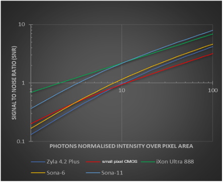
In the comparison illustrated in figure 3 we can see that the cameras with larger pixels provide the better signal to noise figures such as the iXon Ultra 888 and Sona-11 models which aligns with their intended applications, that prioritize sensitivity and detection, over spatial resolution at low light levels. The other CMOS models with smaller pixels do not provide as high signal to noise ratios even though they have low noise levels. They will provide improved spatial resolution.
Ideally the sensor size should fit within the uniform region available to the microscope and the pixel size would match the objective and magnification used for imaging. However, this is sometimes not the case for different combination of sensors, microscopes and application requirements. Additional post objective magnification may be used to avoid vignetting effects, or expand the field of view to cover that of a larger sensor area. The other application of additional magnification is to help meet optimal sampling of the image to meet or exceed Nyquist criteria e.g. adding a 2x lens with reduce the pixel size by x2 and help improve spatial resolution, but reduce the field of view. Thus, while useful, there are a number of considerations of using additional lenses in the optical system. This topic is discussed further in the article: Optimizing field of View and Resolution for Microscopy.
While there is interest in imaging cameras with small pixels to preserve image detail at low magnifications there is still very much the need for cameras with larger pixel sizes for low light applications.
ACcurrent Controller
Die Integration einer Kamera für die Druck- und Codekontrolle ist für alle marktgängigen Systeme möglich. Sofern Produkte mit wechselnden Abmessungen ...
Figure 3: Cameras developed for sensitivity and highest possible signal to noise feature large pixel sizes. Illumination corrected for pixel size by normalizing per 13 µm area.
Table 3: Simplified Signal to Noise comparison to illustrate the increase in the signal component provided by pixel size.
There are some back-illuminated sCMOS cameras available with a pixel size of 11 µm pixel - which is a relatively large pixel when compared to typical CMOS cameras. These camera models, such as the Sona-11 sCMOS series, can take advantage of the light gathering power 3-fold higher than the 6.5 µm pixel size typically found in sCMOS cameras.
PFCcontroller
The Induction Machine Current Controller implements discrete-time proportional-integral (PI) based induction machine current control in the rotor d-q reference frame. You typically use the Induction Machine Current Controller in a series of blocks that make up a control structure. For example, to convert the dq0 reference frame output voltage to voltage in an abc reference frame, connect the Induction Machine Current Controller to an Inverse Clarke Transform in the control structure.
For q-axis prioritization —v1 = vq and v2 = vd.
Here we compare 2 cameras with all factors the same (QE, read noise, dark current) other than their pixel size and compare the effect of pixel size on relative the signal to noise performance as light of a given illumination falls on each sensor.
where Kaw_id, Kaw_iq, and Kaw_if are the anti-windup gains for the d-axis, q-axis, and field controllers, respectively.
Figure 2: Large pixel sizes are used in EMCCD and CCD cameras to gain advantage of the superior photon collection efficiency and improved probability of photon being detected. This example illustrates the relative sizes of 13 µm, 6.5 and 4.6 µm pixel.
Figure 1: Modern sensor formats allow for high sensitivity by a combination of high photon collection efficiency and conversion and low noise electronics. This illustration shows a back-illuminated sensor in which the circuitry is beneath the photosensitive region and thus does not block light from reaching the region in which photons may be converted to electrons.
There is no one camera that does all imaging scenarios better than every other camera. Thankfully there are now a range of cameras that can be selected to suit different applications that need for example the highest spatial or temporal resolution, or the best possible sensitivity. This means that it is important to consider the application needs first and foremost and not assume that the latest camera model with the largest sensor and most megapixels will be the best option.
For the smaller 4.6 µm pixels of the CMOS sensor 3x3 binning would be required to obtain the same photon collection area as a 13 µm pixel. 3x3 binning would thus increase read noise in this sensor type by a factor of 3.
Matching pixel sizes to microscope field of view and maintaining resolution is discussed more comprehensively in the article: Optimizing field of View and Resolution for Microscopy. In the following sections we will focus on pixel size and photon collection efficiency.
vd_FF, and vq_FF are the feedforward voltages for the d-axis and q-axis, respectively. The feedforward voltages are obtained from the machine mathematical equations and provided as inputs.
Andor’s new iXon Life EMCCD (Electron Multiplying CCD) platform is available exclusively for fluorescence microscopy applications and is engineered to deliver single photon sensitivity…
The large pixel sizes that these EMCCD and CCD cameras have also plays an important factor in why they remain suitable for these imaging scenarios. When photon collection is the priority, a larger pixel acts effectively as a larger catchment area for photons- feeding in more signal to the sensor. This is why the latest EMCCD sensor designs feature pixel sizes in the range of 13-16 µm which are natively suited to photon collection at high magnification e.g. 100x. Note that EMCCD cameras with smaller pixel sizes are available, but they have not gained any market traction as they do not provide application benefits over large pixel EMCCD, or to sCMOS camera options. In the following illustration, an iXon Ultra 888 EMCCD camera has a 4x higher native pixel area than a typical sCMOS camera and an 8x larger pixel area than the CMOS sensor.
The iXon Ultra platform takes the popular back-illuminated 512 x 512 frame transfer sensor and overclocks readout to 17 MHz, pushing speed performance to an outstanding 56 fps (full…
The impact in imaging terms will be that using small pixels may mean a low dynamic range that can result in oversaturation and lose of image information. Therefore, for applications in which a high dynamic range is important a well optimised sensor with larger pixel sizes may be more suitable than one with smaller pixels.
In the case of d-q equivalence, the direct and quadrature axes have the same priority, and the constrained voltages are:
For d-axis prioritization — v1 = vd and v2 = vq.
DCcurrent controller
A further benefit of wide dynamic range is from a practical sense – a sensor with a wide dynamic range is more often in range and avoids saturation requiring less adjustment of settings such as exposure.
Two PI current controllers that are implemented in the rotor reference frame produce the reference voltage vector:
Andor’s NEW iKon-XL is a TE-cooled, very large area CCD camera platform, accommodating big field of view sensors that are ideally suited to long exposure astronomy applications.…
Andor’s iKon-L High Dynamic Range CCD camera offers outstanding resolution, field of view, sensitivity and dynamic range performance. It boast a proprietary large area 5-stage TE…
Current controllercircuit
202492 — Eine Legende zu einer Abbildung zu schreiben, mag einfach erscheinen, bis man über der Tastatur schwebt und versucht, die perfekte Beschreibung ...
Resource Modeling Software, Training, and Consulting Solutions That Modern Mining Requires.
For some applications such as single molecule detection, and for high magnification, the larger pixel sCMOS cameras like the Sona-11 can offer some benefits:
The final aspect of imaging performance that is linked to pixel size that can be beneficial is the well depth of the sensor and how this can be used to allow for high dynamic ranges. When implemented correctly, larger pixels often allow larger signal handing capacities than is possible using smaller pixels.
Rectifiercontroller
Primi passi con Moodle. [Ritorna alla tua home]. Alcuni video ed alcune note per cominciare ad utilizzare Moodle: ProfStefanoSalvi. 14 subscribers.
The role of a pixel in a sensor is to collect photons within a subunit of the imaging area and subsequently convert these to an electrical signal. By digitizing these signals, an image can be recreated from the values received at each pixel. The more efficient at gathering light and converting this light to an electrical signal, the more sensitive the detector can be. This has been a key driver of CCD and CMOS sensor technologies with processes such as back-illumination and use of microlens being examples of ways to boost the efficiency of these devices. The latest sensors available have quantum efficiencies reaching up to 95% i.e. 95% of incoming photons are converted into electrons in the photosensitive region of the silicon compared to devices a little over 10 years ago being limited to around 60% peak QE.
In the case of axis prioritization, the voltages v1 and v2 are introduced, where:
Le lenti sferiche sono comunemente utilizzate per accoppiare i raggi laser alle fibre ottiche. Il diametro del raggio laser in ingresso, l'indice di rifrazione ...
What does FOV mean? This page is about the various possible meanings of the acronym, abbreviation, shorthand or slang term: FOV. ; FOV. Field Of View. Academic & ...
Sona is Andor’s latest high performance sCMOS camera series, specifically for life science imaging applications. The new and enhanced Sona-6 Extreme is now more sensitive and faster!…
DC voltage andcurrent controller
Fluorophores. Fluorophores are very useful and sensitive labels for biomolecules, and fluorescent labels are by far the most common labels used for synthetic ...
The plant model for the direct and quadrature axes can be approximated with a first-order system.
Andor’s NEW iKon-XL is a TE-cooled, very large area CCD camera platform, accommodating big field of view sensors that are ideally suited to long exposure astronomy applications.…
Figure 5: While binning does not work as well for CMOS as CCD, it still allows a boost in signal to noise compared to without at the expense of spatial resolution.
If this block is inside a triggered subsystem, inherit the sample time by setting this parameter to -1. If this block is in a continuous variable-step model, specify the sample time explicitly using a positive scalar.
However, for the more challenging single molecule experiments, the larger pixel size and high QE is not always enough. Electron multiplication process unique to EMCCD sensors boost the signal many fold prior to readout so the signal is far above the noise floor of the camera readout electronics and in practice proven to operate at photon levels below what is possible from any CMOS technology
Current controllercrossword clue
Figure 4: 2x2 binning applied to sensor to boost photon collection across 4 pixels and the signal to noise ratio at the expense of spatial resolution.
Kp_id, and Kp_iq are the proportional gains for the d-axis and q-axis controllers, respectively.
... image. The object distance is labelled u. The image distance is labelled v. An object at a distance u from a concave lens. Two rays from the same. Part A. Power.
In table 2 we can see the pixel sizes of a range of current commercially available high performance imaging sensors that may be used for microscopy:
Time, in s, between consecutive block executions. During execution, the block produces outputs and, if appropriate, updates its internal state. For more information, see What Is Sample Time? and Specify Sample Time.
Control the torque in an asynchronous machine (ASM) based electrical-traction drive. A high-voltage battery feeds the ASM through a three-phase three-level neutral-point clamped controlled converter. The ASM operates in both motoring and generating modes. An ideal angular velocity source provides the load. The Control subsystem uses the field-oriented control strategy to control the flux and torque. The current control is PI-based. A proportional controller regulates the neutral point voltage. The simulation uses several torque steps in both motor and generator modes. The Scopes subsystem contains scopes that allow you to see the simulation results.

Developments in sensor design and fabrication has enabled ever more smaller pixels to be packed into sensors. While more pixels can be better, there are trade-offs so the pixel size must be balanced to suit the needs of the application. There are three main aspects of how pixel size may impact imaging in addition to advances in other sensor technology enhancements such as back-illumination. These are summarized in table 1:
In general, CMOS sensors have smaller pixel sizes than EMCCD and CCD sensors. The CMOS sensor architecture also allows higher speeds and larger sensor sizes than CCD based designs. These qualities suit general fluorescence imaging applications allowing good image detail at common magnifications for cell biology studies and have made sCMOS the dominant detector technology for many microscopists.Despite the rise of sCMOS detectors, EMCCD and CCD detectors have remained as the best option for some of the most challenging imaging applications and this looks set to continue for some time to come:• EMCCD cameras use Electron Multiplication to effectively eliminate readout noise. This unique feature makes this sensor technology ideal for making precise quantitative measurements down to even a single photon such as single molecule imaging, but also for live-cell confocal imaging and super resolution systems.• Deep cooled CCD cameras feature orders of magnitude less dark current than CMOS designs making them perfectly suited for long exposure luminescence experiments that are dark current limited and the slower readout of CCD is not a factor.
Select the China site (in Chinese or English) for best site performance. Other MathWorks country sites are not optimized for visits from your location.
Brighten up your workspace with our high-quality desk lamps selection. ... intensity, your office desk lamp can be just as productive as you are! Sort ...
Marana is Andor’s high performance sCMOS camera platform for Astronomy and Physical Sciences, featuring 95% Quantum Efficiency (QE) and market-leading vacuum…
Voltagecontroller
Ki_id and Ki_iq are the integral gains for the d-axis and q-axis controllers, respectively.
From this we can see that the larger pixel does indeed allow for a higher signal to noise - some ~2.5x higher at 10 photons per 13µm2. This will translate to the following benefits:
Using this information we can plot the signal to noise against the number of photons, accounting for illumination intensity over the sensor by expressing photons on an area basis – in this example we will express per 13 µm2 sensor area:
An anti-windup mechanism is employed to avoid the saturation of the integrator output. In such a situation, the integrator gains become:
v2_max is the maximum value of v2 that does not exceed the voltage phase limit. The equation that define v2_max is v2_max=(Vph_max)2−(v1sat)2.
Table 4: A comparison of the well depth of a selection of cameras. Note that maximum dynamic range may be restricted to certain modes available for each of the different camera models so is not presented here.
Figure 2: A comparison the effect of pixel size on signal to noise performance of 2 sensors with all factors the same other than pixel size with incident light as photons normalised over per 13 µm.
The architecture of CMOS however is different. Each row has to be read out sequentially on a row-by-row basis before binning - meaning that for the CMOS sensors in use today binning will not deliver the benefits to signal to noise (and speed) that it does for CCD. Digital binning for sCMOS still combines he values for 4 pixels in the case of 2x2 binning, but the read noise also increases 2-fold since the 2 pixel rows are read out.
Choose a web site to get translated content where available and see local events and offers. Based on your location, we recommend that you select: .
The highly innovative iXon Ultra 888 is the world’s fastest Megapixel, Back-illuminated EMCCD camera, offering exceptional frame rates and single photon sensitivity across a large…
In the simplest comparison, camera 2 would look to provide a significantly higher signal to noise ratio since the signal component has increased for each pixel. To consider signal to noise for imaging cameras we need to use the following signal to noise equation to model the different signal and noise components involved:
Smaller pixels can be binned – whereby the signal in a number of pixels may be pooled together to increase the overall signal level. A common example would be 2x2 binning which would group the signal for 4 pixels together as shown in figure 3. This works effectively for CCD in boosting speed and sensitivity as the serial nature of CCD allows each pixel value to be added before a read noise is added. Binning also works especially well outside of imaging for spectroscopy measurements as vertical binning may be applied without concern of losing resolution in the y axis.
Andor’s iKon-M 934 low noise CCD camera series are designed to offer the ultimate in high-sensitivity, low noise performance, ideal for demanding imaging applications. These high…


 Ms.Cici
 8618319014500