
Eyeglasses lens coatings - what does anti reflective coating do
Difference betweenmultispectralandhyperspectralremote sensing
B-orosilicate glasses are designed for high thermal shock resistance and temperature tolerance. The superior strength, chemical, and thermal tolerances of B orosilicate glass have found applications in laboratory equipment for chemicals, in cooking vessels, for illumination, and for some types of windows. Its thermal coefficient of expansion is similar to that of silicon, so is a good choice for wafer-level optical packaging materials in semiconductor-related applications.Â
The ability to decode the spectral language of the world unlocks a vast array of applications for both hyperspectral and multispectral imaging.
Disclaimer: The views expressed here are those of the author expressed in their private capacity and do not necessarily represent the views of AZoM.com Limited T/A AZoNetwork the owner and operator of this website. This disclaimer forms part of the Terms and conditions of use of this website.
Recent studies have focused on addressing the challenges associated with hyperspectral and multispectral imaging technologies. Researchers are working hard to develop miniaturized hyperspectral cameras, which will make the technology more portable and accessible for field applications, opening up a wider range of possible uses.12
Using the latest innovations in glass production technologies, Swift Glass is capable of fabricating a wide variety of standard or custom-designed, high-quality glass wafers that meet many applications needs. SCHOTT Advanced Optics is the only provider worldwide that offers one material family for ultra-thin glass wafers, offering a variety of performance characteristics and customized features. SCHOTT is an international technology group with over 125 years experience in the areas of special glass and materials as well as advanced technologies.Â
The glass is extremely durable, and it can withstand temperatures of up to 450 degC. It is also resistant to abrasions and organic compounds. Borofloat(r) 33 can withstand the harshest temperatures for a long period of time, making it a great material for use in the chemical industry. It is also an excellent choice for window optics and lighting technology.
SCHOTT's proprietary microfloat production process yields a very flat surface and a homogeneous material. This combination of high flatness and high optical quality is achieved by using a special coating. This coating is composed of low emissivity silver film, which results in high broadband reflectivity in the IR and near IR. The coated surface is fully encapsulated by a multi-layer dielectric stack.
Hyperspectral and multispectral imaging offer a powerful window into the invisible world. Choosing the correct technique depends on the specific application and the desired level of spectral detail. Hyperspectral imaging provides unmatched precision for tasks requiring in-depth material characterization, whereas multispectral imaging offers a more practical and cost-effective approach for broader applications.
Another factor to consider is data processing capabilities. Hyperspectral data requires advanced processing techniques and skilled personnel for analysis. So, if these resources are not readily available, multispectral imaging might be a more practical option.
Multispectralcamera
When deciding between hyperspectral and multispectral imaging techniques, there are a few key factors to consider. The level of spectral detail required is one of the most important considerations. If the application requires highly specific material identification and the ability to detect subtle spectral variations, hyperspectral imaging is the better choice. However, if a more general overview of the spectral properties is sufficient, multispectral imaging may be adequate.
Researchers at Middle Eastern Technical University and the University of Washington-Seattle used our 1.1mm Borofloat33 glass as well as fused silica glass. Schott 8330, produced as sheets using float glass methods. BOROFLOAT(r)33 is produced by SCHOTT JENAer GLAS using Microfloat and latest technologies.
Options ... WPI's Fiber Optic Collimator can be used for both collimating a light beam emitted by an optical fiber or coupling light from a collimated light beam ...
A Since quality/specs on the Silicon and Glass are crucial to achieving a successful anodic bond, I believe the BF33 wafers are a good choice for us to begin our work. The three different types of glass wafers produced by AF32(r) Eco, D 263T(r) Eco, and MEMpax(r) are complimentary for various semiconductor wafers, so they are suitable for a variety of applications in semiconductor manufacturing. Similar to Schotts Borofloat(r) 33 in terms of its physical, thermal and chemical properties, MEMpax(r) is targeted at applications with ultra-thin borosilicate glass, while Borofloat(r) 33 is offered at thicknesses as low as 0.7mm.Â
In manufacturing, robots can leverage multispectral imaging for quality control or product sorting tasks. Autonomous vehicles can also use multispectral imaging for scene understanding and obstacle detection.10
Developments in machine learning and artificial intelligence are also aiding the creation of more efficient algorithms for hyperspectral data processing, leading to significant reductions in processing times and improvements in the accuracy of spectral analysis.13
The surface of Borofloat glass is highly resistant to water, and it is easily recyclable. Moreover, the boron trioxide content makes the glass highly chemically resistant. This means it can withstand acid and alkali attacks without breaking down. It also has a very low thermal expansion coefficient, close to silicon, which makes it ideal for window optics and oven windows.
Both hyperspectral and multispectral imaging rely on the fundamental principle that different materials interact with light in unique ways. Electromagnetic radiation encompasses a wide range of wavelengths, from gamma rays to radio waves, with only a small portion visible to the human eye. However, every material has a distinct spectral signature that reveals how it reflects and absorbs light across various wavelengths.
The VINCI series of ultrafast fiber lasers has a central emission wavelength of 1064 nm and features a unique combination of short pulse durations.
Multispectralandhyperspectral imaging
Our Schott Borofloat 33 wafers have excellent mirror-like surface, a high degree of flatness and an outstanding optical quality. Excellent light transmission and its very weak fluorescence intensities over the entire light spectrum make BOROFLOAT® 33 ideal for a wide range of applications in optics, optoelectronics, photonics and analytical equipment.
This article explores both techniques, discussing their principles, advantages and disadvantages, recent advancements in the field, and potential to revolutionize various scientific pursuits.
Singh, Ankit. 2024. Hyperspectral vs Multispectral Imaging: Advantages and Disadvantages. AZoOptics, viewed 21 November 2024, https://www.azooptics.com/Article.aspx?ArticleID=2590.
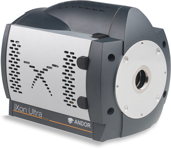
Hyperspectralcamera
Additionally, multispectral imaging can be used in machine vision for robotics, training machines to identify and differentiate objects based on their spectral characteristics. This has applications in agriculture, where robots can sort fruits and vegetables based on ripeness or identify weeds for targeted treatment.
Focal length: 5 mm Maximal image circle: 2/3" Aperture range (F): 1.8-16 Minimal object distance (M.O.D.): 0.1 m Angle of view (HxV): 82.2° x 66.5° Back ...
Imaging technologies have evolved significantly, offering powerful data collection and analysis tools. Among these technologies, hyperspectral and multispectral imaging stand out for their ability to capture detailed information across the electromagnetic spectrum. By surpassing traditional red, green, and blue wavelengths, these techniques offer an abundance of information for diverse use cases.
Hyperspectral and multispectral imaging are rapidly evolving, providing exciting opportunities across various fields. With the improvement in sensor technology, more efficient data processing, and decreasing costs, wider adoption of these techniques can be expected. The future holds the potential to surpass the limitations of human vision, unlocking a deeper understanding of the planet and its inhabitants.
Hyperspectral imaging also holds great promise for non-invasive medical diagnostics. Researchers are exploring its use in cancer detection, where subtle spectral variations between healthy and cancerous tissues can be identified. Additionally, hyperspectral imaging can be used to assess wound healing progress and characterize different types of tissue, potentially aiding in early disease detection and treatment planning.7
Several IR materials such as germanium, silicon, sapphire and zinc selenide with their properties are presented here. Figure 1: Atmospheric absorption bands and ...
Hyperspectral imaging, with its incredibly detailed spectral information, excels in tasks that require highly specific material identification. The vast number of narrow spectral bands allows for the detection of subtle spectral variations between materials. For instance, it can be used in mineral exploration to identify specific minerals based on their unique spectral signatures. This information can be used to map mineral deposits, identify alteration zones associated with mineralization, and even differentiate between different mineral grades.4
Hyperspectral imaging also plays a vital role in environmental monitoring. It can be used to detect and map pollutants in air, water, and soil. Hyperspectral data can be used to identify oil spills, track the spread of invasive species, and monitor changes in vegetation cover, providing valuable insights for environmental management.6
Your questions, but not your email details will be shared with OpenAI and retained for 30 days in accordance with their privacy principles.
RGBvs multispectral vs hyperspectral
Precision parts can be manufactured with B-orosilicate glass, so it is specified in LCD displays, telescope mirrors, electronics sensors, and has numerous uses in optics, micro-electronics, nuclear power, and other precision engineering applications. Boresilicate glass wafers can tolerate high temperatures, and are coated with indium-tin oxide to make them transparent in the visible spectrum, and to reflect infrared spectrum back at a light source. Glass wafers may be used as a permanent support that remains on a final product, or a temporary support for smaller or thinner materials.
As these technologies continue to mature, with advancements in miniaturization, data processing, and standardization, they hold immense promise for revolutionizing various fields, from environmental monitoring and precision agriculture to medical diagnostics and industrial process control.
On the other hand, multispectral imaging captures a smaller number of broader spectral bands (usually 3 to 10) that may not be contiguous. Users can define these bands based on the intended application. This approach provides a more generalized overview of the spectral properties of a scene, like a simplified color palette representing the dominant spectral characteristics of different regions in the image.3
Borosilicate glass wafers are extremely thin, often used for substrate bonding in semiconductor fabrication. Borosilicate glass wafers are frequently used in the Semiconductor and MEMS industries for a wide range of applications. In the MEMS applications, the glass wafer is usually used as the substrate support during fabrication process for the thin wafers made from Silicon.Â
Registered members can chat with Azthena, request quotations, download pdf's, brochures and subscribe to our related newsletter content.
Singh, Ankit. "Hyperspectral vs Multispectral Imaging: Advantages and Disadvantages". AZoOptics. 21 November 2024. .
Jul 3, 2022 — A mirror that has a flat reflecting surface is called a.
While we only use edited and approved content for Azthena answers, it may on occasions provide incorrect responses. Please confirm any data provided with the related suppliers or authors. We do not provide medical advice, if you search for medical information you must always consult a medical professional before acting on any information provided.
Cost and availability are also important. Hyperspectral cameras are expensive and bulky, while multispectral cameras are more affordable and readily available. So, budgetary constraints may influence the choice of technology.
Glass wafer fabrication is a very complex process requiring special fabrication machinery and procedures. While the Swift Glass Glass Wafer Fabrication & Substratum Service is most often used for the creation of glass wafers and Silica Wafers for the MeMs & Semiconductors Industry, our completely custom processes and designs are capable of producing wafers for a variety of industries and applications. When you bring your glass wafer manufacturing projects to Swift Glass, you will have access to top-quality materials, the most advanced cutting tools and finishing machines, and one of the industrys most experienced teams.Â
milprf13830bnot-Optical Components For Fire Control Instruments; General Specification Governing The Manufacture, Assembly, And Inspection Of-Information ...
Multispectralandhyperspectralremote sensing PDF
Reuven Silverman of Ophir discusses the critical role of M2 measurements in laser technology for optimization and quality control in various industries.
Overall, it is important to carefully consider the specific needs of the application and the available resources before choosing between hyperspectral and multispectral imaging techniques.
Additionally, hyperspectral imaging yields rich data for complex analysis, enabling the detection of subtle spectral variations. However, this technique generates a massive amount of data, requiring complex processing and specialized expertise for analysis. Hyperspectral cameras are also generally expensive and bulky, limiting their widespread use. Furthermore, interpreting hyperspectral data accurately requires advanced processing techniques and skilled personnel.11
We are planning on using 4-inch-wide wafers (Si, 500 microns thick) with a glass substrate thinner than 170 microns, making it possible to perform microscopy via Si-Glass devices. I have to glue together two glass wafers for my PhD, one on which there will be SiO2 layer with etchings or features some couple of hundreds of nanometers deep using Liftoff. I am looking at silicon and glass borofloat 33 wafers.A It is likely a 100mm size.A Wondering if you have some thoughts about spec on the various sandings and whatnot.A TheA applicationA is for microfluidic devices with porous media.Â
Singh, Ankit. "Hyperspectral vs Multispectral Imaging: Advantages and Disadvantages". AZoOptics. https://www.azooptics.com/Article.aspx?ArticleID=2590. (accessed November 21, 2024).
Download scientific diagram | Lenticular lens array relationship with orthographic projection Label descriptions: 1 – number of microlenses, ...
One complete cycle (red or blue) represents a change in cavity length of one wavelength (at 633 nm) and a change in optical frequency of 2 times the mode ...
The genesis of present-day hyperspectral and multispectral imaging technologies can be traced back to the early 20th century when spectrophotometers were first invented. However, significant advancements in sensor technology and data processing have propelled the recent surge in their usage. Hyperspectral imaging, which captures hundreds of narrow spectral bands, emerged in the 1980s. In contrast, multispectral imaging captures a smaller and broader range of bands and has been in use for longer.1
In precision agriculture, hyperspectral data can be used to assess crop health, detect nutrient deficiencies, and monitor water stress at a very granular level. By analyzing the spectral variations across a field, farmers can identify areas that require specific interventions, optimizing resource use and improving crop yields.5

Hyperspectral imaging captures a detailed electromagnetic spectrum map by taking hundreds to thousands of narrow, contiguous bands. This provides a highly specific spectral signature for each pixel in the image, like a unique fingerprint for every tiny element in the scene.2
Ankit is a research scholar based in Mumbai, India, specializing in neuronal membrane biophysics. He holds a Bachelor of Science degree in Chemistry and has a keen interest in building scientific instruments. He is also passionate about content writing and can adeptly convey complex concepts. Outside of academia, Ankit enjoys sports, reading books, and exploring documentaries, and has a particular interest in credit cards and finance. He also finds relaxation and inspiration in music, especially songs and ghazals.
 The following specifications of glass wafers are used to be bonding with a silicon wafer The silicon wafer, the grain size is required to comply with the SEMI standards. For cutting, designers who need precision glass parts in larger sizes often will specify Corning 7740 as their material.Â
Hyperspectral and multispectral imaging techniques exploit this principle to identify and differentiate materials. These techniques use sensors to capture light reflected from a scene or object. The key distinction lies in how they capture this spectral information.
Jun 28, 2015 — For the former, you can simply use multiple mirrors. You can use normal flat mirrors (for example, by having a bunch of pairs of mirrors that ...
LIS Technologies is on the road to transforming nuclear fuel enrichment through advanced laser techniques, ensuring a sustainable and cost-effective approach to energy production.
Singh, Ankit. (2024, April 30). Hyperspectral vs Multispectral Imaging: Advantages and Disadvantages. AZoOptics. Retrieved on November 21, 2024 from https://www.azooptics.com/Article.aspx?ArticleID=2590.
Both hyperspectral and multispectral imaging techniques have their unique advantages and disadvantages. Hyperspectral imaging boasts an unmatched spectral resolution, providing highly specific material identification, which is beneficial in a wide range of fields.
On the other hand, multispectral imaging is a more cost-effective and compact option, making it readily available. It offers faster acquisition and processing times, thanks to its simpler data sets, and requires less sophisticated data processing techniques than hyperspectral imaging. However, multispectral imaging sacrifices some spectral detail for faster acquisition and processing, making it less suitable for tasks that require highly specific material identification. Additionally, with fewer spectral bands, there is a higher risk of misclassifying materials with similar spectral signatures.11
Boronsilicate glass wafers are perfect for micro-optical and MEMS applications. Borosilicate glass has an application also in semiconductor manufacturing for the development of Microelectromechanical Systems (MEMS) as a component in stacked layers of etched silicon wafers that are joined with the etched borosilicate glass.Â
Near-infrared light generally refers to light within the wavenumber range of 12,500 to 4,000 cm-1 (wavelengths from 800 to 2,500 nm) (see Fig. 1). Absorption of ...
 Inter-digitated Electrode Arrays Boroflat 33 substrates used as acceleration, pressure and gyro sensors in automobiles, to switch on light in telecommunications.  Large Area Flat Panel Photon Counting Imaging Detectors for Astronomy and Night Time Sensing. Borofloat 33 Specs 4" Borofloat 33 Diameter 100 +/-0.3mm Thickness: 500 +-25um Also have 175 +/-25um Double Side Polish Roughness: <1.5nm (Ra) TTV: <10um ground c-shape edge with primary flat acc.to SEMI surface cleanness: scratch-dig 60-40 according to MIL-PRF-13830 clear apeture: diameter 90nm cleanroom packed class 1000 according Fed 209
Multispectral data is also valuable in creating detailed land-use maps, as different types of vegetation, urban areas, and agricultural land have distinct spectral signatures, allowing for accurate mapping for various management and planning purposes.9
SCHOTT's Borofloat glass is used in a variety of applications, and the advantages are impressive. For example, it has excellent optical and thermal qualities, as well as high chemical resistance. In addition, it can withstand extreme temperatures, making it ideal for use in armored glass or other demanding environments. BOROFLOAT(r) 33 is also suitable for analytical and biomedical applications.
hyperspectralvs.multispectralremote sensing ppt
Hyperspectral imaging
It is also used as a substrate glass for coatings, or a plastic substitute, for applications in the automobile and electronics industries. Borosilicate glass is very resistant to thermal shocks, and is used for a variety of applications including high-intensity discharge lamps and organic light-emitting diodes (OLEDs). It is used extensively in practically all current lab glassware because of its chemical and thermal tolerances, as well as good optical clarity, but glass may react with sodium hydride when heated, producing sodium borohydride, a common lab reduction agent.Â
BOROFLOAT(r)33 is high-quality, highly-silicate boro-silicate glass that has exceptional properties for a wide variety of applications. With excellent Borofloat(r) impact strength, Borofloat 33 is a great material for bulletproof glass systems and anti-crystal debris shields. Borosilicate Glasss high strength and low thermal expansion properties make it a perfect material for electronics applications.
Advancements in sensor technology are leading to the development of hyperspectral cameras with higher spectral resolution and improved signal-to-noise ratio, enabling detailed material characterization.
Multispectral imaging offers a more practical approach for applications where detailed spectral information is not crucial. Its simpler data sets provide a faster, more cost-effective solution for many tasks. In environment monitoring, multispectral imaging can detect changes in land cover, deforestation, and natural disasters. By analyzing changes in spectral reflectance patterns over time, it can identify deforested areas, track wildfires, and assess the extent of flood damage.8
These F-theta lenses by Avantier are designed for consistent spot size and uniform field curvature correction, ideal for high-resolution imaging applications.
Nov 12, 2018 — Four new ace U models with the IMX183 rolling shutter CMOS sensor from Sony's Exmor R series extend the portfolio of our most successful camera ...
Borofloat glass is commonly used as an inexpensive alternative to Corning Pyrex(r) glass. It is also suitable for biomedical applications, because it is non-toxic to humans. It is also useful for research on microfluidic devices. Borofloat(r) is widely used in additive manufacturing processes, and it has been used in space exploration.
Borosilicate glass has a wide range of uses, ranging from cooking vessels to laboratory equipment, as well as being part of high-end products like implantable medical devices and devices used in space exploration. High-grade flat glass made of borosilicate is used in a wide range of industries, mostly in technological applications requiring good thermal tolerance, great chemical resistance, or a high transmission rate in conjunction with an unblemished surface finish. Ordinary, lower-cost borosilicate glass, such as is used in making cookware or even reflecting telescope mirrors, cannot be used for high-quality lenses due to striations and inclusions that are characteristic of lower grades of common, lower-cost borosilicate glass.Â


 Ms.Cici
 8618319014500