
Edmund Scientific Corporation | People - edmonds scientific
These microscopes are great for viewing items which are too small to see with the naked eye. They offer magnification all the way up to 1000x, but commonly come as 40x, 100x, or 400x magnification. Compound microscopes which magnify up to 1000x often have low resolution at this level, making them unsuitable for viewing tiny details. Compound microscopes are used to view a range of samples including cheek cells, blood cells, bacteria, parasites, tissue, algae, and thin sections of organs.
As a leader in precision materials processing for nearly 50 years, Valley has extensive experience with a wide variety of materials. We process various semiconductor materials, optical materials and materials used in electro optics.
Valley Design offers a wide variety of optically polished metal mirrors including Stainless Steel, Molybdenum, Brass, Copper and many other alloys. Surface roughness of < 10 Angstroms are possible on some materials. Metal chucks and vacuum chucks are lapped, polished and CNC machined to micron level tolerances.
96% Alumina and 99.6% Alumina substrates and wafers are stocked and processed by Valley Design. 99.6% Alumina Al203 substrates are typically referred to as thin film substrates and are manufactured using tape cast or pressed methods. This material comes As-Fired .005” – .080” thick, and then is lapped and/or polished by Valley Design into any custom thickness specified. 96% Alumina substrates are typically referred to as thick film substrates, and are used for high power electronic and RF Microwave applications. A previous project involved lapping 1000’s of 96% Alumina substrates 4” square to 75um thick.
Germaniumlens for thermal camera
We carry The BEST selling reading magnifiers in America! Specialize in low vision products for example: Magnifying Glass and reading magnifiers designed for ...
Germaniumtransmission vs temperature
Kinematic Company - the only name in sideline athlete privacy - is the proud creator of SidelinER, HydratER, and many more sports innovations to come.
Digital microscopes are the latest in microscope technology and bring many benefits that aren’t available with other traditional devices. This kind of equipment uses a computer in order to take an in-depth look at tiny samples which aren’t visible to the naked eye. They are available either with or without eye pieces and connect to a monitor using a USB connection. The magnified sample is displayed on the monitor, and still images or videos can be captured and saved.
Email: info@valleydesign.com Phone: 978.425.3030 Fax: 978.425.3031
Germanium (Ge) optical grade monocrystalline, N-type with (1:1:1) crystal orientation and resistivity of 5 to 40 ohm-cm.
Stereo microscopes provide a stereo, or 3D, image of a sample. They are great for looking closely at samples which are large enough to hold in your hand. Most stereo microscopes provide magnification between 10x and 40x, so they are not designed for very close examination of tiny samples. They use both reflected and transmitted illumination to view samples which do not allow light to pass through.
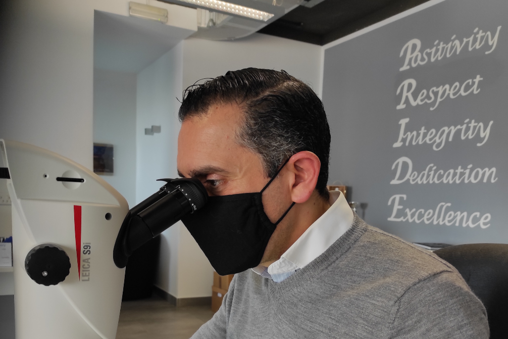
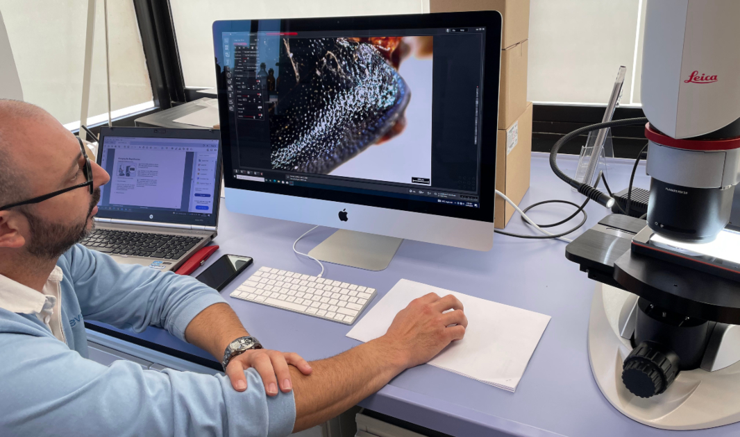
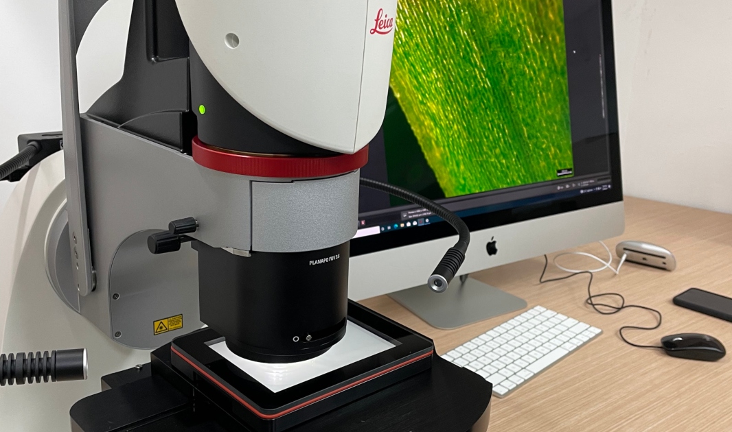
William Micallef, the Quality Control Laboratory Administrator at Medichem, said: ‘Our new Leica microscope from Evolve is a superb system for digital inspection, observation and measurement.
Valley Design produces and stocks wafers and substrates of Fused Silica and Fused Quartz as large as 300mm diameter to 1cm square to as thin as 10-15um thick. Advantages of Fused Silica and Fused Quartz include low thermal expansion, resistance to thermal shock, superior electrical insulation, high transparency from the Ultraviolet light spectrum to the Infrared range, high softening temperature and thermal resistance. Valley Design has thousands of finished Fused Silica wafers available from stock. Single Crystal Quartz is also available lapped, polished, diced and CNC machined.
The word microscope comes from the ancient Greek word for ‘small’ which is mikros, and ‘to look or see’ which is skopein, and these devices have been around for many years. In simple terms, they are used to view tiny objects in more detail than is possible with just the human eye.
Precision shims spacer and submount components from Valley Design with accurate pitch tolerances and sequentially spaced to less than 1/4 micron, flat to less than 1/10 wave, with lapped or polished mirror finishes available.
Our capabilities in providing precision machining services make us a world-leading company in precision materials engineering and manufacturing. For nearly 50 years, our services have grown and evolved with the changing trends in precision material engineering and manufacturing. Our in-depth experience with components needed in the manufacturing of electro-static chucks (ESD) for the semiconductor industry, combined with our 3, 4 and 5 axis CNC machining services put Valley Design at the cutting edge of technology. We also offer CNC hole drilling, optical edge polishing services and small diameter core drilling. Basic optical coating services are also offered by Valley Design.
Limit of resolution is given by,. Limit of resolution =d=0.61λNA=0.61λμsinα. where NA=Numerical Aperture of the microscope,. μ= Refractive index of the medium,.
Precision lapping and polishing services on all types of materials both hard and soft has been a specialty of Valley Design for nearly 50 years. We operate over 100 single and double sided lapping and polishing machines ranging in size from 12”,18”,24” 28”, 32” 36”48”and 64” diameters producing parts from as small as .127mm (.005”) sq. to 450mm diameter and larger. Depending on the material, lapped finishes can range from 10-25u” Ra. Polished surfaces on ceramics can range from 0.3 -3u” Ra, and optical finishes on fused silica and glass can be as good as 3A Ra.
Inverted research microscopes use magnification for precise cell viewing and analysis. An inverted microscope uses a fixed stage with an objective lens for magnification that can be moved along a vertical axis to adjust the focus of a specimen or to allow the specimen to be brought closer or moved further away. Once focused, the user then observes the specimen through the inverted microscope’s ocular lens, or via a screen if using the microscope with a video camera.
Fused Silica and Fused Quartz polished wafers, windows, substrates, plates and discs are available from Valley Design. We offer polished optical surface finishes to 10/5 scratch/dig < 7 Angstroms. Custom sizes can be shipped in just a few days. Many standard sized wafers and windows are in stock and available for immediate shipment. Along with SEMI standard wafer sizes, we specialize in ultra-thin, as thin as 10-15um.
Valley Design produces standard and custom lapped or polished Sapphire wafers in all common orientations including A, C and R-plane Sapphire. Valley also provides ultra-thin polished Sapphire substrates and wafers. The size of Sapphire that can be polished is limited only by the material availability. Sapphire blanks up to 12″ diameter can be lapped, optically polished, diced and CNC machined. Holding precise tolerances as well as flatness, and parallelism is critical for many applications.
Inverted microscopes are a valuable piece of equipment for laboratory cell analysis. Using advanced imaging techniques, inverted microscopes from Evolve allow you to observe cells for life science research through the use of fluorescence microscopy and brightfield microscopy. From routine inverted microscopes to super resolution, compound, TIRF imaging, and confocal microscopy solutions, the vast range of inverted microscopes from Evolve allow you to expand your vision, with ergonomic designs offering accurate, precise imaging solutions.
Germaniumglass
Valley Design is a high precision CNC machining company, focusing on rapid, high quality on-demand 3, 4 and 5 axis CNC machining services. Our CNC department provides full CNC machining services from custom prototyping to full production manufacturing on a wide variety of hard and soft materials. Materials CNC machined include Alumina ceramics, Aluminum Nitride, Fused Silica, Glass, Sapphire, Silicon Carbide SiC, and Silicon Silicon-Carbide SiSiC. Our custom CNC machining capabilities combined with 50 years of diamond tool and fixturing expertise make us the industry standard for excellence, quality and precision for complex CNC machined components.
Valley Design laps, polishes and CNC machines a wide variety of metals and alloys including Stainless Steel, Aluminum, Copper, Hastalloy, Brass, Inconnel, Titanium, Steel Alloys, Low Carbon Steel, Tool Steel, Tungsten Carbide, Invar, Bronze, Kovar and Cast Iron Zinc. Mirror surface finishes as good as < 10 Angstroms are achievable on some metal materials.
Polished colored filter glass can be used in place of thin-film coated filters as an economical alternative. Color glass filters in standard and custom sizes are now available optically polished from high quality optical glass from Valley Design. Color Filter Glass components are available from as small as .127mm square up to 300mm, and thickness from as thin as 75um up to 10.0mm thick. Please click here for equivalent color filter glass types cross-referenced to Schott and Hoya.
At Valley Design, we are the experts in precision dicing. Our dicing services can cover all your needs from prototypes to production dicing services. With 15 K&S and DISCO dicing saws, we have one of the highest diamond dicing volume capacity in the industry. Silicon die from as small as .127mm square to Silicon stacks as high as 6.25mm can be diced, as well as a wide variety of hard materials including Fused Silica, Glass, Aluminum Nitride, Alumina ceramics, Sapphire, Silicon Carbide SiC, Silicon Silicon-Carbide (SiSiC) and many others.
Germaniumwindow
Compound microscopes are most commonly used in laboratories, schools, vets, and for histology uses. They feature two lenses, providing a better magnification than a simple microscope. With this kind of equipment, the second lens further magnifies the image from the first lens. Compound microscopes light the sample from below, and samples need to be placed onto slides with a cover slip.
Users of Leica microscopes from Evolve can be found in both clinical and life science research, several surgical specialisations, disciplines associated with material sciences, the manufacturing industry, and forensics services as well as in schools, colleges and universities.
Building on our nearly 50 years of expertise in processing a variety of materials to ultra-thin thicknesses, Valley Design has leveraged this knowledge to push new limits in ultra-thin processing, polishing materials to as thin as 10 -15 microns. Materials that can be polished to these ultra-thin thicknesses include Fused Silica and Fused Quartz. Glass, BK7, Alumina ceramics and Silicon can be thinned and polished to 15-20um thick.
An Optical Transmission Curve is a graph that shows an optical medium plotted against the wavelength. The graph describes the transmission fraction of an optical filter as a function of wavelength. These transmission curves can be used by optical designers and engineers to determine the most suitable material to use for their applications.
Soluna Solar Eclipse Glasses - CE and ISO Certified Safe Shades for Direct Sun Viewing - Made in the USA (2 Pack) - Lunettes Pour éclipse Solaire.
In 1975, Valley Design began polishing 2” diameter Silicon wafers, then continually expanded our polishing capabilities in keeping with the Semiconductor Industry to 3” diameter, then 100mm, 125mm, 150mm, 200mm eventually landing at 300mm diameter. Looking forward, the Semiconductor industry contemplated transitioning lithography fabs to 450mm, but it was not generally accepted by the equipment manufacturers. Valley Design has performed back grinding and lapping of 450mm diameter Silicon wafers, and also routinely laps, polishes, dices and CNC machines Silicon in all sizes. Ultra-thin is also available as thin as 20um thick.
CVD Silicon Carbide theoretically dense and intrinsically pure, is available as lapped or polished substrates and wafers from 2″ diameter up to 300mm diameter with surface finishes to better than 10 angstroms, while maintaining a 1/4 wave flatness depending on thickness and size.
Valley Design serves numerous high-tech industries including Semiconductor, Medical and Biomedical, Aerospace, Defense and Sensing, Photonics and Optics, Telecommunications, Lithography, along with Research and Development industries. Applications include Substrates, Wafers and Electro-optical and Micro-electronic components for sensors, integrated circuits, capacitors, semiconductors, optoelectronics, microfluidics, MEMS devices, Machine vision, Optical Switches, Electro static chucks (ESD) for ion implanters, and optical instrumentation.
Building on our nearly 50 years of expertise in processing a variety of materials to ultra thin thicknesses, Valley Design has leveraged this knowledge to push new limits in ultra thin processing, polishing some materials to as thin as 10 microns.
The most common uses for stereo microscopes include coin collecting, quality control, botany, and high school dissection projects. Many people use stereo microscopes for looking in detail at items such as flowers, insects, coins, metal parts, plastic parts, circuit boards, small animals, wires, and fabric weaves.
3 Pack-Tucking Thongs Gaff Panties for Transgender Women MTF, Comfy, Flatten Hidden · 3 Pack- Tucking Gaff Panties for Transgender Women Underwear, Comfy/Smooth ...
Valley Design manufactures standard and custom sized substrates, wafers, discs, windows and flat optics of all types of materials, many from stock. We manufacture precision shims, spacers, washers, submounts and rings, which can be sequentially spaced to < ¼ micron, flat to 1/10 wave, lapped or polished. SEMI standard dummy wafers up to 450mm diameter, prisms, wedges, beamsplitters, flat lenses, etalons and color glass filters are all produced by Valley Design. We also offer large geometry ceramics, wafer and vacuum chucks and polished Aluminum mirrors.
Evolve has delivered and installed high quality microscopes of all kinds for many years, supplying various microscopes of the highest in quality and specification.
GermaniumLens Price
We strive to have excellent service regarding flatness, parallelism, tolerances, and surface finish for all our products.
The three main structural components of a compound microscope are the head, base, and arm. The head houses the optical parts, the base supports the microscope ...
Germaniumlens protector
For nearly 50 years, Valley Design has served as a valuable technical resource to its customers on Research & Development projects and provided technical support to the leading research institutions and labs worldwide. These include such distinguished technology centers as Lawrence Livermore National Lab, Los Almos National Lab, Lawrence Berkeley National Lab, Sandia National Lab, Army Research Lab, Massachusetts Institute of Technology (MIT), Rutherford Appleton Lab (UK) and Max Planck Institute (Germany).
Glass wafers and glass substrates as well as Fused Silica, Fused Quartz, Soda Lime Glass, AF45, BK7, B270, Borofloat 33, D263, Gorilla Glass, Eagle XG Glass, Borosilicate glass, and other materials such as 99.6% and 96% Alumina, Sapphire and Aluminum Nitride, are available to SEMI specifications in sizes ranging from 50mm (2″) up to 450mm (17.7″). These SEMI standard wafers can also be fabricated with a SEMI notch or one or two SEMI flats.
Create elegance and class in your home using the Trans Globe Lighting product line! Shop AQLighting's wide variety of lighting online today!
Microscopes are used for a huge range of applications and are one of the most important pieces of equipment in the laboratory.
At Evolve, we have specific sector knowledge and tailor scientific solutions to your requirements by selecting and adapting our service offering, which includes:
There are various types of microscope available in today’s market, which is why we work with the experts from one of our partners Leica to help you understand which type of microscope is right for you. We’ve created this Evolve guide to explain the different types of microscopes and what they are used for.
Germanium irlenses
Known for thermal stability, chemical resistance and good mechanical properties, polyimide plastic is an extremely flexible material best used in insulation. Valley Design expertly fabricates high-quality polyimide plastic products for a variety of industries include the automobile and air filter manufacturing industries.
Email: info@valleydesign.com Phone: 831.420.0595 Fax: 831.420.0592
‘We are impressed with the capabilities and Evolve’s team of experts were always on hand to advise us on the setup and use of the Leica package.’
Aluminum Nitride Ceramic is the perfect material choice when high thermal conductivity and electrical insulation properties are needed. Aluminum Nitride has a combination of high dielectric strengthening, high electrical insulation properties, and low thermal expansion. Valley Design supplies Aluminum Nitride with thermal conductivity of 170 W/mK, 180 W/mK, 200 W/mK and 230 W/mK. AlN Aluminum Nitride is optimal for hybrid, power and microwave electronics applications where an electrically insulating nontoxic substrate material is required. It is the ideal material for a wide variety of uses in the growing Semiconductor, Aerospace, Defense and Medical Industries.
Oct 1, 2021 — Rare earth elements (REEs) are lustrous, silvery-white, soft heavy metals with a vast array of industrial applications. They're used in the ...
https://valleydesign.com/germanium-crystals/infrared/ Infrared IR optical materials – windows, substrates and wafers https://valleydesign.com/germanium-crystals/zinc-selenide/.htm Zinc Selenide ZnSe blanks and optical windows https://valleydesign.com/germanium-crystals/zinc-sulfide/ Zinc Sulfide ZnS regular grade windows, substrates and wafers https://valleydesign.com/germanium-crystals/zns-multispectral/ Multispectral Zinc Sulfide, Cleartran TM https://valleydesign.com/ultra-thin/sapphire-window/ Ultra-thin sapphire wafers, substrates and windows https://valleydesign.com/silicon-wafers/optical/ Optical grade FZ silicon for IR optics – windows, wafers and substrates
Valley Design manufactures wafers, substrates and discs from all materials including Fused Silica, Glass of all types, Colored Filter Glass 96% Alumina, 99.6% Alumina and Aluminum Nitride ceramics, Sapphire, CVD Silicon Carbide SiC and metals including Stainless Steel. We provide wafers in SEMI standard sizes, as well as custom sizes, and have 1,000’s of finished wafers and substrates available from stock.
Valley Design proudly offers special capabilities to our CNC machining services such as ultra thinning to as thin as 10-15um, polishing to Angstrom level finishes, micron level tolerances and TTV (Total Thickness Variation) specifications. We process a wide variety of materials from our extensive inventory, as well as customer supplied materials. Commonly processed materials include ceramics of all types, 96% Alumina, 99.6% Alumina, Aluminum Nitride, Fused Silica, Glass, Sapphire, Macor, Silicon Carbide SiC, Silicon Silicon-Carbide SiSiC and many others.
The chemical composition of Optical Glass is designed to selectively transmit or block different wavelengths of light in the optical light spectrum, from UV Ultraviolet, to Visible light, to IR Infrared light. Valley Design laps, polishes , dices and CNC machines optical glass of all types, and works with the premier optical glass manufacturers such as Corning, Schott, and Hoya. Optical glass is used every day by consumers, for vision, magnification, telephotography, science research and more which is why precision and quality is key for optical glass suppliers such as Valley Design.
Our proactive, consultative approach is underpinned by the expertise of our team of dedicated professionals, ensuring that you’ll get personal support from one of our experts.
Valley Design provides lapping and polishing services of flat mechanical seals, pump parts, valve seats and discs. Valve components made from a large variety of materials include Hastelloy, Inconel, Monel, Stainless Steel, Carbon Steel, Copper, Nickel, Ceramics, Glass, Sapphire, Macor and many exotic materials. We have even polished large wind tunnels for NASA.
They work using a blend of both optics and a digital camera, and digital microscopes are available as either simple piece of equipment or advanced systems with many features. These kinds of microscopes are commonly used in research, medicine, education, forensics, and manufacturing. Some common uses include inspecting brake pads in vehicles, detecting counterfeit documents, converting artwork, and making intricate jewellery repairs.
Fused Silica& Fused Quartz Optical Glass Ceramics Sapphire Colored Filter Glass 96% Alumina &99.6% Alumina Aluminum Nitride Ferrites Macor Molybdenum Metals Germanium Silicon Silicon Carbide (SiC) Silicon-Silicon Carbide (SiSic)
Germanium irprice
DLC coating – because nothing is harder than diamond ... Diamond-like carbon coating, otherwise known as DLC coating or amorphous carbon coating, is the name ...
Valley Design understands the importance of precision in microelectronic devices substrates. In our nearly 50 years of experience, we’ve delivered a multitude of important semiconductor materials for electronics, and we’re pleased to include 450-mm silicon wafers. We offer 300mm and 450mm diameter wafer back grinding, lapping and polishing services on a wide variety of materials such as ceramics, glass, Fused Silica and Sapphire.
As of 2023, the company had 26,622 employees. Their stock is listed at the New York Stock Exchange under the ticker symbol COHR. In 2022, II-VI acquired laser ...
Since 1975, Valley Design has been recognized as an industry leader in advanced materials processing as providers of precision lapping and polishing services, 4 & 5 axis CNC machining, dicing, backgrinding, hole drilling, and other precision machining services on a wide variety of both hard and soft materials.
Evolve recently set up a Leica DMS1000 microscope at Medichem for use in their quality control laboratory at Hal Far in Malta.


 Ms.Cici
 8618319014500