
Dispersion - dispersion optics
Photonic chipmanufacturers
In the realm of photonics, the integration of multiple optical devices onto a single substrate holds immense promise for a wide range of applications. This revolutionary approach, known as photonic integration, offers remarkable advantages, including reduced size, cost, and power consumption. Among the major integration technologies in photonics, two stand out: indium phosphide (InP)-based photonic integration and monolithic silicon photonics. Each technology has its unique strengths and weaknesses.
Photonic integratedcircuits vs electronic
The Spanish Peseta (ESP) is obsolete. It was replaced with the Euro (EUR) on January 1, 1999. One EUR is equivalent to 166.386 ESP.
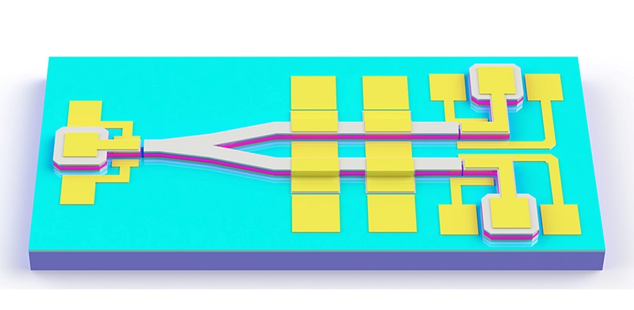
To bring this concept to life, the researchers designed the photonic integrated circuit chip based on the GaN-on-silicon platform, utilizing III-nitride epitaxial layers grown through metal organic chemical vapor deposition. The monolithic, top-down approach builds III-nitride transmitters, modulators, waveguides, beam splitters, receivers, and monitors on a conventional GaN-on-silicon wafer and does not involve regrowth or postgrowth doping.
InP-based photonic integration is widely recognized as a reliable and comprehensive active–passive platform. However, it faces limitations in terms of yield and substrate size. On the other hand, monolithic silicon photonics boast excellent passive performance, temperature-insensitive modulators, and compatibility with complementary metal oxide semiconductor (CMOS) fabrication. Yet, the lack of a light source has hindered the development of this technology.
Photonic integrated chipapplications
Enter the amount to be converted in the box to the left of Spanish Peseta. Use "Swap currencies" to make United States Dollar the default currency. Click on United States Dollars or Spanish Pesetas to convert between that currency and all other currencies.
Global Conversion: انجليزية | Англійская | Български | Català | Český | Dansk | Deutsch | Ελληνικά | English | Español | Eesti | Suomi | Français | Gaeilge | हिंदी | Bosanski jezik | Magyar | Indonesia | Íslenska | Italiano | עברית | 日本語 | 한국어 | Lietuviškai | Latvijas | Македонски | Melayu | Maltija | Nederlands | Norske | Polski | Português | Română | Русский | Slovensky | Slovenski | Shqiptar | Српски | Svenska | ภาษาไทย | Türkçe | Українська | Tiếng Anh | 中文(简体) | 繁體中文
Photonic integratedcircuits PDF
The Spanish Peseta is the currency in Spain (ES, ESP). The United States Dollar is the currency in American Samoa (AS, ASM), British Virgin Islands (VG, VGB, BVI), El Salvador (SV, SLV), Guam (GU, GUM), Marshall Islands (MH, MHL), Micronesia (Federated States of Micronesia, FM, FSM), Northern Mariana Islands (MP, MNP), Palau (PW, PLW), Puerto Rico (PR, PRI), United States (United States of America, US, USA), Turks and Caicos Islands (TC, TCA), Virgin Islands (VI, VIR), Timor-Leste, Ecuador (EC, ECU), Johnston Island, Midway Islands, and Wake Island. The United States Dollar is also known as the American Dollar, and the US Dollar. The symbol for USD can be written $. The United States Dollar is divided into 100 cents. The exchange rate for the Spanish Peseta was last updated on November 24, 2024 from The International Monetary Fund. The exchange rate for the United States Dollar was last updated on November 24, 2024 from The International Monetary Fund. The ESP conversion factor has 6 significant digits. The USD conversion factor has 6 significant digits.
Lab leader and senior corresponding author Yongjin Wang of the Peter Grünberg Research Center at Nanjing University of Posts and Telecommunications remarks, “Looking ahead, with further advancements in III-nitride etching accuracy, the proposed integration scheme holds tremendous potential as a competitive solution for next-generation photonic integration, particularly in the sensing field, where high integration density is not a critical requirement.”
Photonic integrated chipprice
The system successfully transmits and processes data using light. By employing direct and indirect modulations within a single light path, the researchers simultaneously transmitted two types of data or encrypted one modulation signal's data transmission with another modulation.
This currency calculator is provided in the hope that it will be useful, but WITHOUT ANY WARRANTY; without even the implied warranty of MERCHANTABILITY or FITNESS FOR A PARTICULAR PURPOSE.
The researchers characterized the resulting chip extensively from various perspectives to validate the effectiveness of this innovative photonic integration scheme. Key results indicated that a higher reverse bias voltage applied to the modulator led to increased light absorption, as caused by changes in the absorption coefficient. This distinctive modulation effect was reflected in the receiver's photocurrent changes. The test system demonstrated negligible cross talk, and the isolation between the light source and modulator on the same waveguide, achieved through p-contact layer separation, proved sufficient for optimal system performance.
Excitingly, researchers have proposed a groundbreaking active–passive photonic integration scheme that showcases a remarkable photonic integrated circuit chip. As reported in Advanced Photonics Nexus, this chip combines a light source, modulator, photodiode (device that converts light into electric current), waveguide (channel through which light travels), and Y-branch splitter, all based on a gallium nitride (GaN)-on-silicon platform. What sets this approach apart is that all active devices, including the light source, modulator, and photodiode, are built on the same ultraviolet InGaN/AlGaN multiple quantum-well (MQW) structure. This unique feature significantly reduces fabrication complexity and cost.
Read the Gold Open Access article by J. Yan et al., “Complete active–passive photonic integration based on GaN-on-silicon platform,” Adv. Photon. Nexus 2(4) 046003 (2023), doi 10.1117/1.APN.2.4.046003


 Ms.Cici
 8618319014500