
Collimated Beams – divergence, laser ... - collimated
GoPro remains headquartered in San Mateo, California, and employs most of its 1,500 or so workers—now including Barna—in the United States.
CMOS Cameraprice
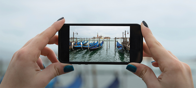
Cell phone cameras, which require tiny, highly efficient image sensors, ended up being the main driver for the mass production of CMOS active pixel sensors. Whenever you take a picture with your phone—or, nowadays, virtually any other digital imager—you’re using NASA technology.
Just as his first image sensor could be built using manufacturing processes that were well-established more than 20 years ago, Fossum is designing this next-generation imaging chip to be compatible with the enormous existing CMOS camera industry. “For factories building CMOS sensors, I think it will be pretty easy for them to switch to the Quanta Image Sensor if they want to do that,” he says.
He notes that cell phone cameras, which would likely not be possible without CMOS imaging, have also had an enormous cultural impact, bolstering the rise of social media, raising questions about police conduct, and bringing awareness to uprisings and crises around the world. “These things can be documented because people are all carrying around cameras,” he says. “The impact went well beyond expectations.”
cmossensor vs full-frame
As that industry drove Micron and others to turn out more and more CMOS imagers every year, resulting improvements to the technology and its manufacture drove costs down and quality up until CCD-based devices couldn’t compete, even where size and power weren’t priorities.
The LibreTexts libraries are Powered by NICE CXone Expert and are supported by the Department of Education Open Textbook Pilot Project, the UC Davis Office of the Provost, the UC Davis Library, the California State University Affordable Learning Solutions Program, and Merlot. We also acknowledge previous National Science Foundation support under grant numbers 1246120, 1525057, and 1413739. Legal. Accessibility Statement For more information contact us at info@libretexts.org.
CMOS-enabled cell phone cameras gave rise to the “selfie” phenomenon, as well as a broader culture of online photo and video sharing. Here, President Barack Obama poses for a selfie with science popularizers Bill Nye, left, and Neil deGrasse Tyson, right. Image courtesy of the White House

“It was sort of the breakthrough spinoff that showed we could do tech transfer out of JPL, too, not just Caltech,” says Fred Farina, the university’s chief innovation and corporate partnerships officer. “So it was the pioneer, in terms of spinoffs out of JPL.”
Anticipating heavy competition, in 2001 the founders sold Photobit to Micron Technology, which could bring more resources and manufacturing capability to bear. By then, the company—and subsidiary Photobit Technology Corporation, created to handle custom-design contracts—had built a healthy business for itself, and CMOS’s takeover of the imaging industry had begun.
When Photobit was sold, the original patents returned to Caltech, which still holds the intellectual property rights that haven’t yet expired, and the world’s top image sensor suppliers, such as Sony and Samsung, license the technology. Meanwhile, Micron spun off its image-sensing business into a company called Aptina, which ON Semiconductor purchased in 2014 for about $400 million.
Fossum was an expert in CCD technology—it was why JPL hired him in 1990—but he believed he could make digital images with smaller and lighter machinery using CMOS technology to create what he called active pixel sensors (APS) (Spinoff 1999, 2002, 2010).
CMOS sensors also allow both the device and the battery to be smaller, and small size is one of GoPro cameras’ strongest selling points. The company’s devices are designed to be mounted, usually on the body, to capture action sequences in video or still images, some at up to 240 frames per second.
\[ A^{2}=\int_{-\infty}^{+\infty} e^{-x^{2}} d x \int_{-\infty}^{+\infty} e^{-y^{2}} d y=\int_{-\infty}^{+\infty} \int_{-\infty}^{+\infty} d x d y e^{-\left(x^{2}+y^{2}\right)}.\]
CMOSimage sensor working principle
Fossum says he was pleased that CMOS allowed the United States to recapture a portion of the imaging market, however briefly, before much of it was lost again to Japan, South Korea, and China. “Micron, GoPro, Omnivision, and a host of others generated tens of thousands—if not hundreds of thousands—of jobs in the United States because of this technology,” he says.
The following year, Fossum left JPL to become the company’s full-time technological lead. In addition to designing custom sensors, Photobit licensed technology to companies like Kodak and Intel, although most of those early licenses didn’t lead to product lines. By 1997, however, CMOS was being taken seriously, and several companies invested in Photobit, including Schick Technologies, which also obtained—and still holds—an exclusive license for CMOS for dental imaging (Go To).
“It was a great example of a truly disruptive technology,” he says, noting that CMOS did not yet perform as well as CCD imagers, but the potential to improve was clear. In addition, it promised to be easier to use with far lower power and could be more cheaply manufactured, he says.
At the last step we have written A2 as a two-variable integral over the entire plane. This seems perverse, because most of the times we work hard to reduce two-dimensional integrals to one-dimensional integrals, whereas here we are going in reverse. But look at the integrand again. When regarded as an integral on the plane, it is clear that we can regard x2 + y2 as just r2, and this suggests we should convert the integral from Cartesian (x, y) to polar (r, θ) coordinates:
CMOSsensor
CMOS technology in general had improved since earlier attempts at using it for image-sensing, and Fossum hit on an approach to reduce the signal noise that had plagued earlier imagers, applying a technique called intra-pixel charge transfer with correlated double sampling—something already used in CCDs. Using this technique, he measured a pixel’s voltage both before and after an exposure. “It’s like when you go to the deli counter, and they weigh the container, then weigh it again with the food,” he explains. The sampling corrected for the slight thermal charges and transistor fluctuations that are latent in photodetector readout, and it resulted in a clearer image.
called the Gaussian integral, does not fall to any of the methods of attack that you learned in elementary calculus. But it can be evaluated quite simply using the following trick.
Barna says the video industry switched to CMOS cameras with the advent of high-definition video. To shoot video with so many pixels on a CCD-based camera would require dramatically more power, draining batteries and quickly overheating the machine, he says. “You would only be able to take very short bursts, and it wouldn’t be the same experience at all.”
Types ofcmos in camera
Fossum, who was inducted into the National Inventors Hall of Fame in 2011, now teaches engineering and entrepreneurship at Dartmouth College’s Thayer School of Engineering, where he is working on what he believes will be the next revolution in digital imaging. His Quanta Image Sensor would cram a billion pixels, each designed to sense a single photon, into an array no larger than those in current CMOS imagers, significantly enhancing low-light sensitivity.
Because CMOS pixels are signal amplifiers themselves, they can each read out their own signals, rather than transferring all the charges to a single amplifier. This lowered voltage requirements and eliminated charge transfer-efficiency issues. And it had the added benefit of allowing almost all the other camera electronics to be integrated onto the computer chip with the pixel array using conventional CMOS production processes, a development that would make CMOS-APS imagers more compact, reliable, and inexpensive.
But by far the widest use of the small, low-power cameras enabled by CMOS technology has been in cell phones. “Cell phones became the ‘killer application,’” Fossum says. “Battery life and camera size are very important on a cell phone.”
Imaging devices based on metal oxide semiconductor devices had been attempted since the 1960s, but no one had ever succeeded in making the technology marketable. The little signal amplifiers had long been used in computer circuitry, but imagers using CMOS as sensors suffered from signal noise, among other problems.
By 1993 Fossum and his team knew they were onto something that could be huge for NASA missions and consumer electronics alike, but as they took their findings on the road, giving talks and publishing papers, they met with resistance from the digital imaging industry and even colleagues at JPL. Fossum attributes this skepticism both to earlier failures in CMOS imaging and to people’s instinct to protect their own livelihoods.
He’s designing the sensor with the assistance of one of his PhD candidates, an experience that in some ways mirrors his early days at NASA. “I had some great organizational mentors at JPL,” Fossum says. “Personally, I loved working for JPL—best job ever.”
Instead, a different imaging technology, using sensors based on the charge coupled device (CCD), allowed high-quality digital photography to come of age by the late 1980s. These image sensors comprise an array of photodetecting pixels that collect charges when exposed to light and transfer those charges, pixel to pixel, to the corner of the array, where they are amplified and measured.
Despite early doubts about CMOS’s potential, several companies signed Technology Cooperation Agreements with JPL and partnered with Fossum and his colleagues to develop the technology.
The action camera company GoPro takes maximum advantage of the small size and high efficiency of CMOS digital image sensors, using the technology to build tiny, high-definition video cameras that users can affix to themselves, selfie sticks, or surfboards to capture their adventures in high fidelity.
Cmos in cameraiphone
For Caltech, the financial returns from the licensing, which fund research and education, are only part of the benefit of the CMOS success story, Farina says. “This helps motivate other researchers at Caltech and JPL, and for the whole culture of entrepreneurship it’s really powerful to have good stories.”
GoPro cameras, which leverage the small size and high efficiency of NASA-invented CMOS active pixel sensors, were originally conceived as surfboard-mounted video cameras, an application that remains popular today. Credit: Kat Patterson
CMOSfull form
By 2013, more than a billion CMOS image sensors were manufactured every year, and by 2015, the technology’s market, which also includes applications in the automotive, surveillance, and medical industries, reached nearly $10 billion.

This page titled 10.2: B- Evaluating the Gaussian Integral is shared under a CC BY-SA license and was authored, remixed, and/or curated by Daniel F. Styer.
“People told me, ‘You’re an idiot to work on this,’” Eric Fossum recalls of his early experiments with what was at the time an alternate form of digital image sensor at NASA’s Jet Propulsion Laboratory (JPL).
CMOSvs CCD
While Photobit held an exclusive license to the technology developed at JPL and filed more than 100 of its own patents, company leadership was concerned that defending its intellectual property would prove difficult as several electronics giants began developing their own CMOS imagers.
Before Photobit was sold, its sensors had made their way into webcams made by Logitech and Intel, as well as ingestible “pill cameras” that are still offered by Given Imaging as a noninvasive endoscopy technique. “I feel very good about that one,” Fossum says of the so-called PillCam. “It’s still used. It’s become a huge industry.”
That same year, Sandor Barna, now vice president of core technologies at GoPro, finished his graduate degree and took a job as an engineer at Photobit.
Digital single-lens reflex cameras, better known as DSLRs, were also early adopters of CMOS technology, which allowed bursts of rapid shots at high resolution.
While CCD sensors are capable of producing scientific-grade images, though, they require a lot of power and extremely high charge-transfer efficiency. These difficulties are compounded when the number of pixels is increased for higher resolution or when video frame rates are sped up.
His invention of the complementary metal oxide semiconductor (CMOS) image sensor would go on to become the Space Agency’s single most ubiquitous spinoff technology, dominating the digital imaging industries and enabling cell phone cameras, high-definition video, and social media as we know it.
The very idea of digital photography was dreamed up at JPL by engineer Eugene Lally in the 1960s. Now the concept of a digital camera on a chip shared the same birthplace.
In 1995, Fossum became the first JPL scientist to license his own invention from the California Institute of Technology (Caltech), which manages the lab, as he, his then-wife and JPL colleague Sabrina Kemeny, and two other JPL coworkers founded a company, Photobit, to develop custom sensors. Caltech’s Technology Transfer Office was created that year, and the office granted Photobit an exclusive license.


 Ms.Cici
 8618319014500