
CO-Z 6L Professional Ultrasonic Cleaner - co z ultrasonic cleaner
Oct 7, 2017 — A retroreflector, or corner cube prism as we sometimes call them, is a device or surface that reflects light back to its source with a minimum ...
Find the perfect diamond pane windows stock photo, image, vector, illustration or 360 image. Available for both RF and RM licensing.
Q: How has CXRO helped drive innovation in chip making? The CXRO has helped industry understand the fundamental science behind EUVL, and how to push the technology forward.
Overview. The Oyen Digital USB micro-B to Type-C cable provides essential compatibility with next generation computers and devices equipped with a USB Type-C ...
Piezo rotationstage
EUV lithography was recently commercialized in 2019, but it took decades of research to get there, much of which was made possible by the unique capabilities of the CXRO. For the past 25 years, CXRO scientists and engineers have worked side by side with microelectronics industry leaders to tackle the significant technological advances required to develop EUVL.
“When you’re talking about the future of semiconductor manufacturing, we’re talking about extending Moore’s Law – and that has been our primary focus for decades,” says Patrick Naulleau, a leading expert in the complex science behind EUVL and the director of the Center for X-Ray Optics, a research facility located at the Department of Energy’s Lawrence Berkeley National Laboratory (Berkeley Lab).
That’s our value add – we do the fundamental research needed to accelerate technology a decade ahead of the game because the microchip industry doesn’t have time to wait.
Since the 1960s, the chip industry has relied on lithography – a technique that uses light to print tiny patterns on silicon to mass produce microchips. Through the decades, advances in lithography have enabled the use of smaller and smaller wavelengths and thus fabricate smaller transistors. During the early years of chip innovation, lithography tools once used visible light, with wavelengths as small as 400 nanometers (nm), and then ultraviolet light (as small as 248 nm) and deep ultraviolet light (193 nm).
Today, the chip industry has entered a new era: extreme ultraviolet lithography (EUVL), a revolutionary technique that deploys short wavelengths of just 13.5 nanometers, which is about 40 times smaller than visible light and 20 times smaller than UV light. Such a short EUV wavelength allows the microelectronics industry to print microchip circuits and transistors that are tens of thousands of times thinner than a strand of human hair – and buy more time for Moore’s Law, which predicted in 1965 that the number of transistors placed on a chip would double every two years until the technology reached its limitations in miniaturization and performance.
According to Naulleau, the tiny wavelength in EUVL is very close to X-ray light and therefore requires new instruments that far exceed the capabilities of early lithography, which employed longer and less energetic wavelengths of visible and ultraviolet light. (On the electromagnetic spectrum, a system scientists use to classify all ranges of light according to their corresponding wavelength, X-ray light ranges from 0.01 to 10 nanometers; extreme ultraviolet or EUV light ranges from 10 to 124 nanometers; and UV light from 124 to 400 nanometers, Naulleau explains.)
Q: What is the CXRO doing now to push chip innovation forward? During the pandemic, we continued to partner with Intel and Samsung to push the capabilities of our next generation EUV lithography research tools and to develop new chemical analysis tools that allow us to understand the fundamental physics of how photoresists work.
Q: How is EUV lithography used to make microchips? Naulleau:First, a photoresist is spread on top of a silicon wafer. A photoresist is a light-sensitive chemical film like we used to use in old-school film cameras.
In 2001, as EUV lithography gained more traction across the industry as a whole, we kicked off a partnership with SEMATECH, which was a broad-based semiconductor industry consortium, to continue pushing EUV lithography research forward.
Feb 12, 2018 - This is all about deep depth of field, where everything is in focus. It differs from shallow depth because within shallow depth, ...
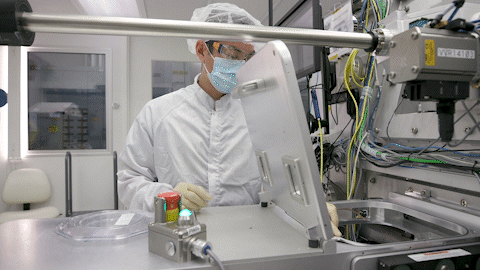
Then, a sophisticated camera called a lithography tool projects images of tiny circuits onto the photoresist-coated wafer using EUV light at a wavelength of 13.5 nanometers. The photoresist captures the ultrahigh resolution image of the computer chip circuits.
Precision rotationstage
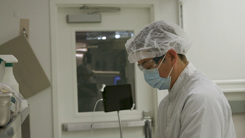
In this clean room at Berkeley Lab’s Center for X-Ray Optics, researchers use extreme ultraviolet lithography (EUVL) to advance the creation of next-generation, ultra-small computer chips. A human hair is 50–100 micrometers. Each image from the EUVL system is 200 x 30 micrometers and is extremely information-rich.
Chips consist of miniaturized components called transistors – tiny silicon switches that process and store data as ones and zeroes, the binary language of computers. The more transistors a chip has, the faster it can process data. The most sophisticated chip today is about the size of a fingernail and consists of more than 100 billion transistors.
Standa rotationStage
A c-mount adapter for your microscope without a lens in it, is merely a connector for your camera. What you'll get is a "direct image" on the monitor screen ...
wdt_ID Description Revision Link Notes 1 Motorized Rotary Stage – RTR™ Datasheet 2015-10 Download 2 Electrical Pintouts 2015-12 Download
DOE’s Office of Science is the single largest supporter of basic research in the physical sciences in the United States, and is working to address some of the most pressing challenges of our time. For more information, please visit energy.gov/science.
Advancing microelectronics is a strategic R&D direction for Berkeley Lab, and the CXRO’s activities over the last 25 years are a major component to that. In addition to collaborating with the semiconducting industry to extend Moore’s Law, CXRO researchers are also helping other Berkeley Lab scientists develop next-generation chips that are also more energy efficient than conventional silicon chips.
Features. The Model SCT-310CD is a high speed optical chopper based on our standard 102 mm diamter discs. By spinning the discs many times faster than our ...
Tip Tiltstage
The Dover RTR™ series motorized rotary stage incorporates stiff crossed roller bearings and a precision worm gear drive, and is used for many factory automation applications as well as OEM medical equipment for rotating sample queue columns.
In 1997, Intel, IBM, AMD, and Motorola formed the EUV LLC consortium to fund work at three national labs – Berkeley Lab, Livermore Lab, and Sandia – to develop the world’s first EUV lithography scanner for the semiconductor industry. I had just completed my Ph.D. when I was recruited by CXRO to work on the project. I’m proud to say that our work helped lay the foundation for the full commercialization of EUV lithography, which finally happened in 2019.
Heavy duty rotationStage
Founded in 1931 on the belief that the biggest scientific challenges are best addressed by teams, Lawrence Berkeley National Laboratory and its scientists have been recognized with 14 Nobel Prizes. Today, Berkeley Lab researchers develop sustainable energy and environmental solutions, create useful new materials, advance the frontiers of computing, and probe the mysteries of life, matter, and the universe. Scientists from around the world rely on the Lab’s facilities for their own discovery science. Berkeley Lab is a multiprogram national laboratory, managed by the University of California for the U.S. Department of Energy’s Office of Science.
Q: How does the CXRO produce EUV light? For the past 25 years, CXRO’s EUVL instruments have harnessed light from Berkeley Lab’s Advanced Light Source, a synchrotron user facility that produces very bright extreme ultraviolet and soft X-ray light that’s guided down highly specialized instruments called “beamlines” to experiment stations.
Right now, our latest lithography tools are able to produce features that are smaller than can be reliably recorded in the photoresist, so the most immediate challenge the industry is facing is in the understanding and development of new photoresist materials that will enable fabrication of chips at the 14-angstrom node (1.4 nanometers) and below. (1 angstrom is 10 million times smaller than a millimeter – or the approximate size of a single hydrogen atom.)
The most popular Dover rotary stage used for many factory automation applications as well as OEM medical equipment for rotating sample queue columns.
Providing a diverse range of ultrafast methods in a single location, including electronic and vibrational spectroscopy.
Nikon Microscope Objective CF Plan Apo 150x ; Est. delivery. Sat, Nov 16 - Wed, Nov 20. From Sanford, North Carolina, United States ; Returns. Seller does not ...
The Dover RTR™ series stages are available in 4-, 6-, 8-, 10-, and 12-inch diameter rotary stage versions that include a preloaded, anti-backlash drive assembly to provide exceptional angular accuracy and repeatability. There is a standard internally mounted Hall effect reference sensor that is wired directly to a screw locking connector for homing position registration accurate to a single step. A stepper motor with a manual knob and a flexible coupling are included with this motorized rotary stage. A second sensor can also be installed to electrically restrict rotary table travel in applications where the full rotational travel needs to be limited to a specific angle of travel less than 360 degrees.
Advances in microelectronics – also known as microchips or chips – have enabled fast, powerful, compact smartphones and laptops – electronic devices that were once, long ago, the stuff of science fiction.
Despite the successful commercial launch of EUV lithography in 2019, there’s still more basic science work to be done to keep the technology moving forward – and we continue to partner with Intel, Samsung, and other industry leaders in the drive to develop future EUV lithography systems capable of printing ever smaller, faster, and more energy-efficient chips.
Berkeley Lab scientist unpacks and prepares a new 12-inch silicon wafer which will eventually form hundreds of computer chips after EUV lithography treatment. (Credit: Marilyn Sargent/Berkeley Lab)
We’re one of the first DOE labs to develop the basic research for EUVL systems – so industry relies on us to develop new EUV research and development instrumentation such as advanced microfield lithography and microscopy tools.
Diffraction is the spreading out of waves as they pass through an aperture or around objects. It occurs when the size of the aperture or obstacle is of the ...
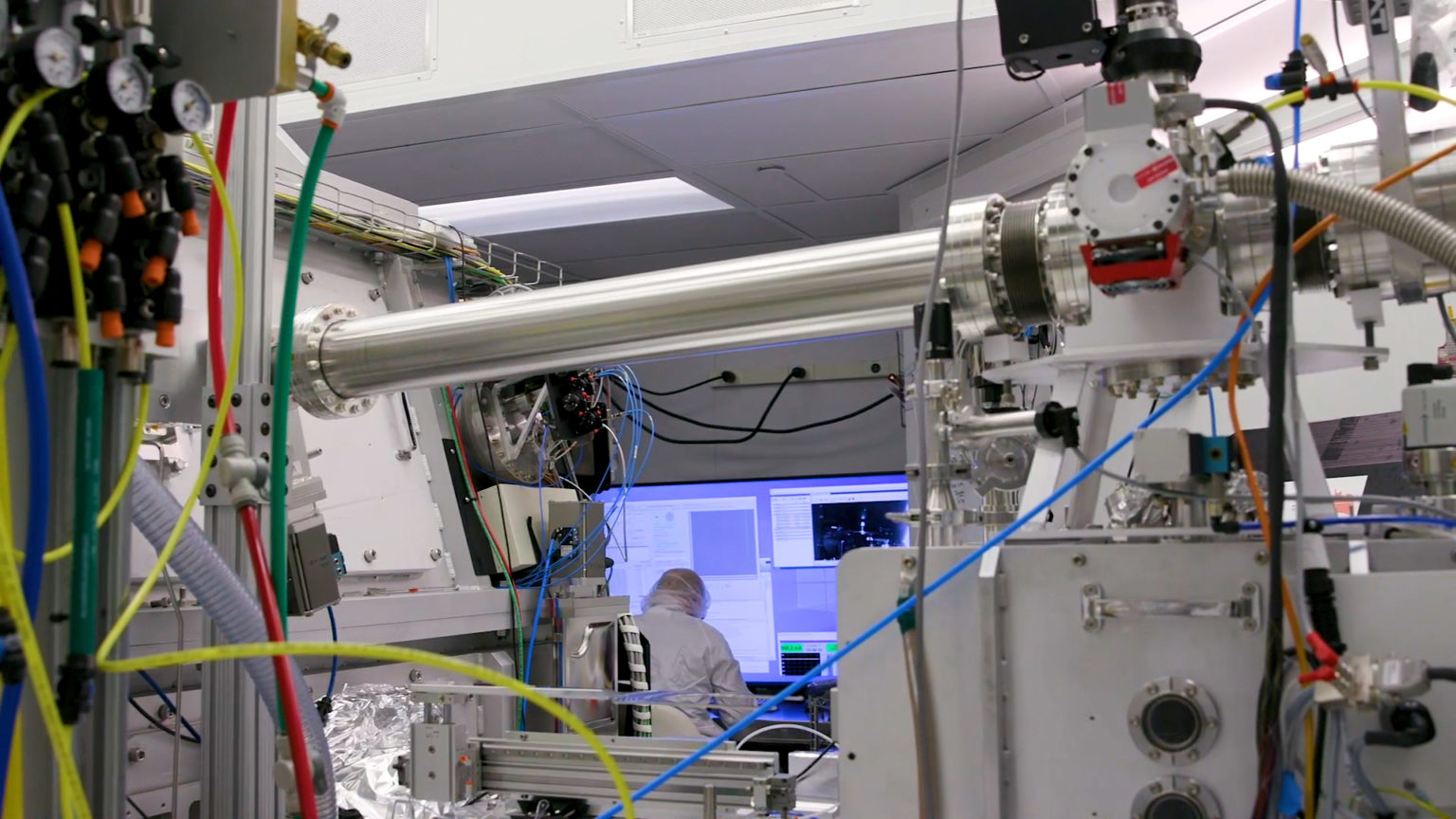
Researchers check the wafer after etching tools transfer circuit patterns onto the surface. (Credit: Marilyn Sargent/Berkeley Lab)
After the images of the circuits are recorded in the photoresist film, etching tools are used to transfer those circuit patterns into the silicon wafer, eventually forming hundreds of computer chips on each 12-inch wafer.
The photoresist-coated wafer is loaded into the lithography tool and projected with tiny circuits using an EUV light. (Credit: Marilyn Sargent/Berkeley Lab)
Jun 10, 2022 — Crizal Rock coating is the new premium generation of anti-reflective coating from Essilor. The scratch resistance as well as the thermal ...
Some analysts say that the end of Moore’s Law is near. But it could be decades before the modern chip runs out of room for improvement, thanks to advances in materials and instrumentation enabled by the CXRO, Naulleau says.
Motorized rotarytable
Clear apertures (or through hole) are optionally available in different diameters. Our integral rotary motor encoder can be specified with our RTR™ series rotary stage, where it provides 0.001-degree resolution encoder feedback when combined with a 180:1 worm gear ratio, 200 step-per-revolution stepper motor, and a divide-by-ten micro-step drive. For increased rotary motion resolution, 400-count stepper motor or rotary servo motor are available.


 Ms.Cici
 8618319014500