
B-Tech AV Mounts - B-Tech International - mount technical
Photonic chipmanufacturers
For the community, the new Edmunds Center will provide a gathering space for youth camps, musical concerts, and other events. In the past, the Edmunds center has hosted Jay Leno, Don McLean, and Hank Williams Junior. The new expansion will present new opportunities for performers and musical acts to inspire and connect with the West Volusia community.
Photonic integratedcircuit components
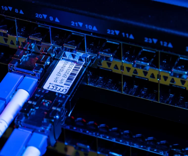
Chip fabrication is a process with many sources of variability, and therefore much testing is required to make sure that the fabricated chip agrees with what was originally designed and simulated. Once that is certified and qualified, the process of packaging and assembling a device with the PIC follows.
Photonics is one of the enabling technologies of the future. Light is the fastest information carrier in the universe and can transmit this information while dissipating less heat and energy than electrical signals. Thus, photonics can dramatically increase the speed, reach, and flexibility of communication networks and cope with the ever-growing demand for more data. And it will do so at a lower energy cost, decreasing the Internet’s carbon footprint. Meanwhile, fast and efficient photonic signals have massive potential for sensing and imaging applications in medical devices, automotive LIDAR, agricultural and food diagnostics, and more.
Photonic integratedcircuits vs electronic
The process of making photonic integrated circuits is incredibly long and complex, and the steps we described in this article are a mere simplification of the entire process. It requires tremendous amount of knowledge in chip design, fabrication, and testing from experts in different fields all around the world. EFFECT Photonics was founded by people who fabricated these chips themselves, understand the process intimately, and developed the connections and network to develop cutting-edge PICs at scale.
At this time, we are still fundraising for phase two which will require gifts of all sizes to complete the renovation. Gifts can be made HERE. If you have any questions or would like more information about the Edmunds Center renovation project, please contact Associate Athletic Director for External Operations, Heather McCormick at hmccormick@stetson.edu Stetson Athletics and the university would like to thank all supporters and donors who have been gracious enough to support our efforts to make the Edmunds Center into a redefined events and entertainment space for Volusia County. Full renovations are expected to be completed by Summer 2025. About Stetson University Athletics: Stetson University's Athletics Program is driven by a shared purpose. It is what inspires, motivates and binds us together. More than a task, a reason for being. THE HATTER PURPOSE is to create and provide an experience of a lifetime through teamwork and relationships to achieve excellence. This purpose is achieved through five Core Values: Communication, Integrity, Excellence, Value People and Commitment. To learn more about the HATS program and our Core Values, visit GoHatters.com/HATS.
Photonic integratedcircuits PDF
Building off the excitement of a successful 2023-2024 basketball season which saw the Women make the NIT and the Men's team make it to March Madness this new home of Hatter basketball is sure to pave the way for future success. New locker rooms will enhance the student athlete experience and provide coaches with new resources and amenities to boost player performance and recovery.
Photonic integrated chipapplications
Given its importance, we want to explain how photonic integrated circuits (PICs), the devices that enable all these applications, are made.
Stetson Cheer, Cross Country, and Volleyball will also benefit from the updates with new locker rooms, and amenities to improve the game/race day experience for the Hatters as well as giving each team a proper space to call their own.
Photonic integratedcircuit market
Photonic integrated chipprice
We ask that you consider turning off your ad blocker so we can deliver you the best experience possible while you are here.
Photonicchips vs semiconductor
While packaging, assembly, and testing are only a small part of the cost of electronic systems, the reverse happens with photonic systems. Researchers at the Technical University of Eindhoven (TU/e) estimate that for most Indium Phosphide (InP) photonics devices, the cost of packaging, assembly, and testing can reach around 80% of the total module cost. There are many research efforts in motion to reduce these costs, which you can learn more about in one of our previous articles.
Especially after the first fabrication run of a new chip, there will be a few rounds of characterization, validation and revisions to make sure the chip performs up to spec. After this first round of characterization and validation, the chip must be made ready for mass production, which requires a series of reliability tests in several environmental different conditions. You can learn more about this process in our previous article on industrial hardening. For example, different applications need different certification of the temperatures in which the chip must operate in.
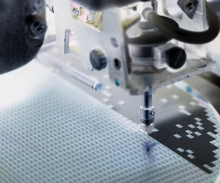
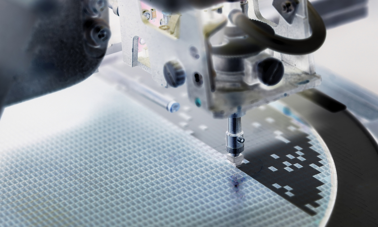
Yuqing Jiao, Associate Professor at the Eindhoven University of Technology (TU/e), explains the fabrication process in a few basic, simplified steps:
Manufacturing semiconductor chips for photonics and electronics is one of the most complex procedures in the world. For example, back in his university days, EFFECT Photonics President Boudewijn Docter described a fabrication process with a total of 243 steps!
Figure 6 summarizes how an InP photonic device looks after the steps of layer epitaxy, etching, dielectric deposition and planarization, and metallization.
The process of designing a PIC should translate an initial application concept into a functioning photonics chip that can be manufactured. In a short course at the OFC 2018 conference, Wim Bogaerts from Ghent University summarized the typical PIC design process in the steps we will describe below.
Real life is, of course, a lot more complicated and will require cycling through these steps tens of times, leading to processes with more than 200 total steps. Let’s go through these basic steps in a bit more detail.
© 2024 EFFECT PHOTONICS All rights reserved. T&C of Website - T&C of Purchase - Privacy Policy - Cookie Policy - Supplier Code of Conduct


 Ms.Cici
 8618319014500