
10x10 White Door Window - 10x10 window
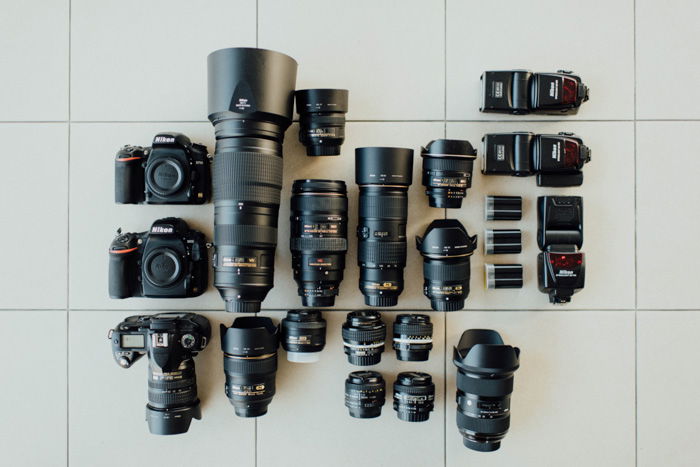
This is crucial because no single lens will ever be able to satisfy the needs of all photographers. Interchangeable lenses empower us to achieve exactly the results that we want.
Nowadays, charge-coupled devices(CCD camera sensors) and complementary metal oxide semiconductor technology (CMOS) imagers make up the majority of sensors.
Lens mount cameracanon

Because the speed at which electrons are moved around a sensor increases read noise, CCDs move electrons much slower than their maximum potential speed.
A full-frame CCD sensor is a kind shown in Figure 2, although there are also additional designs known as frame-transfer CCD and interline-transfer CCD.
The sensor’s ability to transmit data as either a voltage or a digital signal to the following stage will depend on whether it is CCD or CMOS.
They are amplified using the EM Gain register, sent to the output node, converted to a voltage, grey levels, and then displayed with a PC.
The information transferred to the following stage by the sensor will be either a voltage or a digital signal, depending on whether it is a CCD or CMOS sensor.
EMCCDs are far more sensitive than CCDs thanks to the combination of large pixels, back illumination, and electron multiplication.
The image processing sector is currently one of the global businesses with the fastest growth rates, and as a result, it is a crucial area of engineering study.
For sensitive, quick imaging of a range of samples for several applications, quantitative scientific cameras are essential. Since the invention of the first cameras, camera technology has developed significantly.
Photons hit a pixel, are converted to electrons, and then to the voltage on the pixel. Each column is read out separately by individual ADCs and then displayed with a PC.
This technology’s lack of sensitivity and speed constrained the number of samples that could be scanned at acceptable levels.
The RF mount is the newest continuation of EF. It’s almost identical electronically but has a shorter flange distance of 20mm. It adds extra available features, such as a control ring on lenses for changing aperture or ISO. EF and FD lenses are fully adaptable to RF mount.
Electrons go from the image array to the masked array, and then onto the readout register in a manner that is remarkably similar to frame-transfer CCDs.
A mirror mechanism increases the minimum required flange distance for a camera system. If a camera has a mirror, flange distance can’t be much shorter than 45mm. Mirrorless cameras can go as low as 16-18mm.
The images are processed by imaging software on this node, amplified to readable voltage, and transformed into digital grey levels using an ADC.
According to Skyquestt, With a projected size of USD 16.25 billion in 2019 and a projected growth rate of 9.6% during the forecast period (2024–2031), the image sensor market is expected to reach USD 39 billion by 2031 from USD 16.36 billion in 2023.
From consumer to computer vision to industrial, defense, multimedia, sensor networks, surveillance, automotive, and astronomy.
Compared to CCD/EMCCD technology, this combination enables CMOS sensors to operate parallel and analyze data more quickly.
When Sony designed the E-mount, they completely revamped the communication protocol. This caused huge problems when they tried to adapt A-mount lenses (their previous mount).
Customers building next-generation camera sensor products for various applications may rely on Camera Image Processing to provide the best solutions.
The EM Gain register now becomes the primary point of distinction. Impact ionization is a technique EMCCDs to drive more electrons out of the silicon sensor size, doubling the signal.
When you detach a lens, you’ll notice contact pins on both the lens and the camera. They aren’t there for fun: they provide proper communication.
Lens mount cameranikon
The market for complementary metal-oxide semiconductors, or CMOS and sCMOS image sensors, has grown significantly in recent years.
According to datahorizzonresearch, the market growth of CMOS and sCMOS image sensor market size was valued at USD 23.3 Billion in 2023 and is expected to reach a market size of USD 40.8 Billion by 2032 at a CAGR of 6.4%.
Lenses mounted with a bayonet fit perfectly, and there’s only one way to attach a lens. This is essential for electronic communication between a camera and a lens since the contact pins must align properly.
Without the container, an integrated sensor is only the sensor’s fundamental technology. It enables various sensor technologies to be “integrated” or combined into a single plug-and-play component.
In mirrorless cameras, lenses can go almost until they hit the sensor. Most of them don’t, because the rear glass element would be very vulnerable on a lens like that.
3D Imaging: There are now more uses for CMOS image sensors in augmented reality, industrial inspection, and healthcare thanks to their development of 3D imaging capabilities.
A shorter flange distance allows lenses to be designed closer to the sensor. Not only does this free up space, but it also removes the need for some special lens elements.
The change encouraged Nikon to demonstrate power, so they released a 58mm f/0.95 lens. If you’re interested in buying one, expect to spend more on it than on a small car.
The primary purpose of these sensors is to produce images for digital cameras, digital video cameras, and digital CCTV cameras.
Manufacturers sometimes use similar solutions throughout their different lens mounts. The Canon RF mount has the same base pin layout as the EF mount, along with some extra pins. Because of this, adapting EF lenses on R bodies does not compromise their autofocus speed and accuracy.
Bestlens mount camera
A quick tip: if you encounter a communication error in your camera, try cleaning the contact pins. Most of the time this solves the problem.
It depends on two things. Generally, you can adapt lenses that have a flange distance at least 3-4mm longer than the mount you want to adapt it to. The extra distance is needed to fit the adapter itself.
After being exposed to light and changing from photons to photoelectrons in a CCD, the electrons are transported down the sensor row by row until they reach the readout register, which is not exposed to light.
Image Processing: The digital data is routed to the image processor (5), where it is subjected to several enhancements and modifications, including sharpening and color correction.
It is divided into four categories, such as contact image sensor (CIS), charge-coupled device (CCD) image sensor, front side illuminated (FSI), backside illuminated (BSI), and complementary metal oxide semiconductor (CMOS) image sensor.
While CCD and EMCCD technologies were popular for scientific imaging, sCMOS technology has emerged in recent years as the best option for imaging in the biological sciences.
By selecting the best camera manufacturer technology for your imaging system, you can enhance all aspects of your studies and conduct quantitative research.
These neural networks will be able to detect suspicious behavior and transmit an alarm in real time, instead of depending just on motion detection.
Moreover, barcode readers, astronomical telescopes, and scanners all use these electronic chips. Low-cost consumer gadgets are possible thanks to CMOS’s inexpensive manufacture.
Most mount systems contain cameras of multiple sensor sizes. For instance, EF, F and E mounts all support both full frame and APS-C cameras. In those cases, the mount is designed and calibrated for full frame sensors. EF and F were even developed before the cropped sensors’ era.
Additionally, each ADC has to read out considerably less data than a CCD/EMCCD ADC, which must read out the complete sensor because there is an ADC for every column.
In order to freely swap lenses, there must be a standardised connection protocol. Every lens (within a family) must be designed with similar characteristics. Most importantly, with the exact same design on the rear end to fit perfectly to the camera.
Several different locking types exist. Screw lock, breech-lock and bayonet-type lock are the three most important. The first two were (and some still are) used with manual-only lenses. M42 is the most popular screw mount. It’s a universal mount, used in countless cameras and lenses released after the ’50s.
This is the distance between the rear lens element and the sensor. It’s measured at the closest focusing distance since that’s when the lens is closest to the sensor.
Bayonetlens mount
The Canon FD mount was released in 1971. It has a flange distance of 42mm. When the new EF mount was released (with a flange distance of 44mm) this posed a problem. Direct adaptation was not possible without corrective optics. Canon released a teleconverter/adapter, but it only worked with select telephoto lenses.
These electrons can be moved pixel by pixel anywhere on a sensor by employing a positive voltage (orange) to transfer them to another pixel.
Likewise, every camera body has to be designed with an identical lens-attaching surface. This connection is called the lens mount.
If you ever wondered why you can’t easily interchange lenses between different manufacturers, this article is for you. What stops this simple act is the different lens mounts.
Also, camera manufacturers generally want to have their own lens mounts, which they don’t share with anyone else. This ensures that they have full control of development, and won’t have to give out potential business secrets.
The transformation of light photons into electrons is the first process for a sensor (known as photoelectrons). Quantum efficiency (QE), which is displayed as a percentage, is the efficiency of this conversion.
For example, Nikon’s new Z 14-30mm f/4 lens is not only small, but it also boasts a surprisingly great image quality. Yet, its price is reasonable.
A pixel (blue squares) is struck by photons (black arrows), which are then transformed into electrons (e-), which are then stored in a pixel well (yellow).
Lens mountindex
An integrated circuit that is sensitive to light and uses photons and electrons to create images is called a charge-coupled device, or CCD. Pixels are separated from the image elements using a CCD sensor.
Different systems require mounts with different sizes, flange distances, electronic connections, and other physical traits.
The behavior of the readout electronics serves as the integration’s boundary, which is unrelated to the shutter’s exposure.
Lens mounttypes
Bayonet mounts use tabs that lock the lens. Typically, you need to align a colored dot on the lens to another dot on the camera body. The lens needs a turn of 45-90 degrees to lock.
Large format works very differently from smaller formats. In many aspects, it represents 19th-century technology (which doesn’t mean it’s inferior). As such, there is no standardised lens mount on large format cameras. The lens is attached to a lensboard, which is then attached to the bellows.
As CMOS sensors have a far lower read noise than CCD/EMCCD, they can work with weak fluorescence or live cells and move electrons much slower than the projected maximum speed.
The most important one is what sensor(s) it’s designed for. Intuitively, you don’t need such a large mount for a 1″ compact sensor as for a full frame sensor.
Signal Conversion: An electrical signal that could be weak is produced by the sensor. Analog electronics (3) increase this signal by amplifying it.
On a sensor, electrons can be carried in any direction in this way, and they are often moved to a location where they can be amplified and turned into a digital signal, which can then be presented as an image.
CCD sensor Works – Camera Sensor TechnologiesThe above image explains the Different types of CCD sensors. The full-frame sensor is also displayed. Grey areas are masked and not exposed to light.
EMCCD Fundamentals – Camera Sensor TechnologiesThe above image explains, How an EMCCD sensor works. Photons hit a pixel and are converted to electrons, which are then shuttled down the sensor integration to the readout register.
For example, if a CCD detects a signal of 10 electrons with a read noise of 5 electrons, the signal could be read out at any value between 5 and 15 electrons, depending on the read noise.
Some of them were the predecessors of the mounts that we use in modern DSLRs. Some of them went extinct, and some of them are still in use.
An image signal processor (ISP) is a processor that receives a raw image from the image sensor and outputs a processed version of that picture (or some data associated with it).
ExpertPhotography is a participant in the Amazon Services LLC Associates Program, an affiliate advertising program designed to provide a means for sites to earn advertising fees by advertising and linking to amazon.com.
Medium format cameras have shrunk significantly in size. And the need for compactness inevitably brought the need for standardisation.
Camera Lens Mountadapter
The image sensor in a camera system receives incident light, or photons, that have been focused by means of a lens or other optics.
To deliver a high-quality image for a specific camera sensor and use case, an ISP could carry out several procedures, including black level reduction, noise reduction, AWB, tone mapping, color interpolation, autofocus, etc.
Obtaining the ideal image or video quality is tricky for each use scenario. A lot of filtering and iterations are necessary to attain a desirable outcome.
The choice of the appropriate camera sensor has become extremely important and varies from product to product because cameras have a wide variety of uses in many industries.
Along with brand-specific mounts (Canon’s old FD, Nikon F), universal mount types also gained ground. M42, M39 and T-mount are the most notable among these.
When an EMCCD receives a signal of 5 electrons, and the EM Gain is set to 200, the output node will receive a signal of 1000 electrons.
Temporary Storage: Processed photos may be stored in the camera’s buffer (6) indefinitely while they wait to be written to the memory card.
After you twist it to its correct position, a spring-loaded pin locks the lens into place. When you press the lens-detaching button, the pin retracts and the lens can be freely removed.
Photons hit a pixel, converting to electrons that move to the sensor’s readout register, then to the output node where they become voltage, then grey levels, and finally displayed on a PC.
Camera lens mountchart
Also, in general, the wider the mount is compared to the size of the sensor, the more headroom lens designers have. This means that they can design lenses with wider apertures and better image quality.
The other barrier is electronic control if it’s a thing you want. Electronic adapters are much more expensive than dummy adapters. They have chips inside to code and decode the data between the camera and the lens. Still, even the most advanced adapters reduce autofocusing speed slightly.
Optical imaging systems often generate panchromatic, multispectral, and hyperspectral imagery using visible, near-infrared, and shortwave infrared spectrums.
Machine vision covers flat panel displays, PCBs, semiconductors, warehouse logistics, transportation systems, crop monitoring, and digital pathology.
So, when developing their full frame mirrorless mount, they decided to jump to the top. The new Z-mount has the largest inner diameter of any full frame mount currently, 55mm.
On the other hand, Nikon (apparently, as this is not official) redesigned their pin layout on the Z-mount. Adapting directly pin-to-pin is thus not possible. In consequence, the F-to-Z adapter slows autofocusing slightly. There is an even worse example.
The current generation of intelligent devices, which represent a quantum jump in sophistication, is made possible by camera competence.
Light entering a digital camera through the lens hits an image sensor. The camera processes the signal that the image sensor outputs to produce image data, which is then saved on the memory card.
The development and spread of consumer electronics with imaging capabilities underscore the increasing importance of camera image processing.
The growth behind these image sensors is due to the growing need for high-performance, low-power, and reasonably priced imaging solutions across a range of industries.
CMOS sensor technology allows for greater speeds due to its parallel operation, unlike CCD and EMCCD which rely on different methods of sequential operation.
Due to its ability to be multiplied up above the noise floor as many times as needed, EMCCDs can now detect tiny signals.
This implies that positive voltages can attract electrons, making it possible to move electrons across a sensor by applying a voltage to particular sensor regions.
The sensor collects light and transforms it into an electrical signal that is subsequently processed to create a digital image, much like the retina in a human eye does the same thing by translating light into nerve impulses that the brain can understand.
All electrons have a negative charge that underlies the operation of all the sensor types covered here (the electron symbol being e-).
High-Resolution Sensors: There is a growing trend towards higher resolution CMOS image sensors, enabling sharper and more detailed images.
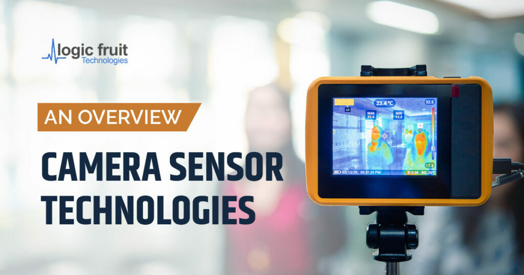
To evaluate the camera sensors’ tuning, image quality, and image resolution, various types of labs tools are required, such as;
These pins are not the same on every lens mount. In fact, they sometimes vary even within a lens mount. For example, the EF mount has seven pins by default. But, some L-series EF lenses have three more to work with teleconverters. EF-mount cameras have 10 pins to accommodate all options.
This was accomplished in several ways via EMCCDs. The cameras’ back illumination (which raises the QE to over 90%) and massive pixels (16-24 m) significantly raise their sensitivity.
EMCCDs provide quicker and more sensitive imaging than CCDs, making them ideal for photon counting or low-light imaging devices.
Users can select a number between 1 and 1000 to have their signal multiplied that many times in the EM Gain register as part of this step-by-step EM process.
Usually, there’s something before the sensor that a glass element can hit, if designed improperly. In DSLRs, it’s the flip-up mirror. In SLT-type cameras, it’s the pellicle mirror.
This includes camera integration, camera image processing, CMOS image sensor technology tuning, and other related capabilities.
This significantly limits them with F-mount lenses. Canon manufactures f/1.0 (discontinued) and f/1.2 lenses with autofocus. Nikon’s fastest F-lenses start at f/1.4. This is solely due to the narrow mount.
The basis for how digital cameras take and create images is thus the camera sensor, which is essential in transforming light into digital information that can be further processed and saved.
The improvements in technology allowed them to get smaller and smaller. Large format photography, where it all started, required a film size of several inches across. Today, smartphone camera sensors only measure a few millimetres.
This implies that the pixel converts a photon into an electron and that the electron is then instantly changed into a readable voltage while still on the pixel.
Due to inadequate illumination and other environmental factors, the captured image may contain some unnecessary elements despite each specific sensor, processor, and lens combination.
The incident light (photons) is focused by a lens or other optics and is received by the image sensor in a camera system.
There was no physical limit to the adaptation. Yet, protocols differed so much that adapted lenses were useless. Autofocusing was impossible, and light metering was problematic, too. The issue was fixed months later with several consecutive software updates.
Digital Conversion: After being amplified, the signal is passed to an analog-to-digital converter (4), which changes it into digital data that the camera can process more easily.
Camera makers use the bayonet mount because of its advantages compared to other types. Attaching and detaching lenses is a faster process than with any other type. It can also be done with one hand, which is crucial when running-and-gunning.
The frame-transfer sensor has an active image array (white) and a masked storage array (grey), while the interline-transfer sensor has a portion of each pixel masked (grey).
CMOS sensors use an on-chip analog-to-digital converter (ADC) to transform photons into electrons, voltage, and finally a digital value.
Hasselblad introduced their lens mount with the 1600F model. It’s still in use today. Others followed, including Pentacon (Six) and Mamiya (645). These are the most popular medium format mounts.
Take the example of Nikon. Their F-mount (first used in 1959) is the narrowest among major full frame DSLR mounts. Its inner diameter measures only 44mm, compared to 46mm on Sony E and 54mm on Canon EF.
The sensor collects light and transforms it into an electrical signal that is subsequently processed to create a digital image, much like the retina in a human eye does the same thing by translating light into nerve impulses that the brain can understand.
There are two major types of image sensors: CCD, or charge-coupled device, and CMOS, or complementary metal oxide semiconductor.
The first is, of course, size. Cameras with shorter flange distances can be much smaller, as their mount doesn’t have to stick out far away. But their image quality can be better, too. This is not because of the cameras themselves. Instead, it’s because of the lenses.
Therefore, in addition to having a lot of pixels, factors like drive technology, quantum efficiency, and pixel size structure all impact imaging performance in different ways.
Mounting direction varies among manufacturers. Most of them attach clockwise, with the notable exception of Nikon’s F and Z mounts. Nikon lenses attach counter-clockwise, and their zoom and focus rings are inverted as well.
Camera Sensor integration, image sensor integration, and camera image processing methods are widely utilized in various applications
ExpertPhotography is part of several affiliate sales networks. This means we may receive a commission if you purchase something by clicking on one of our links.
One is the EF-S mount, which is physically identical to the EF. It allows the mounting of all EF lenses, plus newly-designed crop sensor lenses. EF-S lenses protrude deeper into the mirror box of Canon cameras. They have a shorter back focus distance. This enables Canon to design smaller and cheaper crop sensor lenses.
Every pixel is transformed into an electrical charge, the strength of which is correlated with the amount of light it was able to collect.
A sensor transforms a physical event into a quantifiable analog voltage, or occasionally a digital signal, which is then sent for reading or additional processing or transformed into a display that is readable by humans.
The other one is the EF-M mount, which is smaller than the standard EF. It also has a slightly different communication protocol. It has an 18mm flange distance It was designed for Canon’s smaller M-series mirrorless cameras before the full frame EOS R came out. Adapting EF and FD lenses to M cameras is possible without complications.
AI Transforming Photography: Camera technology is being revolutionized by AI and machine learning, with possible uses ranging from improving image authenticity to countering bogus AI-generated photos.
You may ask: why are then multiple types of lens mounts, why isn’t one enough? For sure, it would be simpler for the end-user.


 Ms.Cici
 8618319014500