
Bright Vision Consulting - brite vision
For high throughput, PCB inspection must be integrated with automated material handling systems like conveyors, robots, or rail-guided carts. Software interfaces between the inspection systems and manufacturing execution system enable seamless and efficient quality control workflows.
dcs官网
PCB inspection not only prevents shipping defective boards, but the data collected enables process improvement by identifying the root causes of issues. In light of rising quality demands and manufacturing complexity, this guide aims to equip engineering and quality control teams with the knowledge to leverage inspection at every stage – from bare boards to fully assembled PCBAs. Implementing the strategies here will reduce risks and costs while accelerating time-to-market.
The DCS-BIOS Hub only knows how to get the name of the currently active aircraft from DCS, which is not very useful. To teach it to interact with a specific aircraft in DCS, you need to install a module definition plugin.
Click âPluginsâ in the navigation menu on the left, then click âOpen the plugin catalogâ. You will see a list of recommended plugins for the DCS aircraft modules that DCS-BIOS has found on your hard drive:
dcsworld破解
AOI systems use high-resolution cameras to capture images of a PCB surface, which are digitally processed to inspect traces, spacing, hole sizes, and other design features. The optical images are compared to an electronic CAD file to identify any discrepancies or defects. AOI inspection can find tiny flaws undetectable by visual inspection. Large-area AOI systems can quickly scan entire panels of multiple PCBs. The speed and accuracy of automated optical inspection make it the most commonly used method for verifying bare PCB quality.
After clicking the start menu shortcut, you will find a new icon in your system tray. If you just installed DCS-BIOS, the icon will probably be hidden; you will have to click the arrow to show hidden icons. If you want Windows to always display the icon, you can drag it onto the taskbar.
Eagle Dynamics
Printed Circuit Board Assembly inspection focuses on verifying soldering quality, component placement, and assemblies on completed PCBs. Some key inspection methods include:
Before assembly, all the components must be inspected to ensure they meet specifications and are free of damage. This includes checking component dimensions, leads, markings, as well as electrical performance and function. Verifying component quality reduces defects introduced in later assembly processes.

Implementing the proper inspection techniques at each manufacturing stage ensures any defects or issues are caught early before they become costly problems down the line. However, maximizing the value of inspection also requires considering additional factors like sampling strategies, data management, and integration with automation. By leveraging the various inspection methods covered here and optimizing their inspection program, PCB fabricators and assemblers can deliver superior quality products to their customers in a consistent and cost-effective manner.
Having a master inspection checklist ensures consistency and prevents overlooking any critical inspection items. Checklists can be customized for each specific PCB product and assembly process.
With this new section, the article now provides a more complete overview of key PCB inspection methods as well as the equipment needed to implement them. Please let me know if you would like me to expand or refine this section further.
You should now be looking at a web browser showing the DCS-BIOS Hub web interface. If that is not the case, verify that your firewall is not blocking the DCS-BIOS Hub from listening on TCP port 5010.
DCS
Production Volume: High-volume production lines benefit from automated inspection methods like AOI and ICT due to their speed and consistency. In contrast, low-volume or prototype production may rely more on manual inspection methods.
A PCB inspection checklist helps ensure all critical steps are covered. Here is a general checklist covering key parameters and defects to inspect for:
In addition to understanding available inspection techniques, implementing an effective PCB inspection program requires considering several other factors:

As a leading PCB manufacturer in China, JHYPCB provides high-quality PCB fabrication and assembly services with 100% PCB inspection. Leveraging advanced inspection equipment and processes, JHYPCB delivers reliable, high-performance PCBs tailored to your requirements. Contact JHYPCB today to experience the quality difference of 100% inspected PCBs for your next project!
After soldering, AOI is used to check component placement and solder joints. High-resolution cameras can rapidly and accurately identify issues like missing components, misalignments, insufficient solder, shorts, or faulty connections. 3D AOI provides detailed imaging for inspection of complex solder joints.
Proper PCB inspection identifies defects introduced during manufacturing and assembly, preventing functional issues or field failures down the line. However, selecting the right inspection techniques can be challenging with the diversity of PCB types, components, and potential defects. By understanding available methods from visual checks to automated optical, x-ray, and flying probe inspection, PCB designers, fabricators, and assemblers can implement an inspection program that cost-effectively verifies quality requirements.
Modern inspection systems generate massive amounts of data. Effective software tools are essential for collecting, storing, analyzing, and reporting inspection results. Statistical analysis of inspection data also provides vital feedback to improve manufacturing processes.
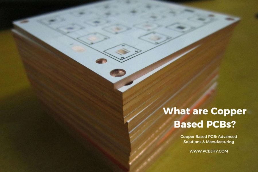
Printed circuit boards are the foundation of electronics. They provide the mechanical structure and electrical connections for components in devices ranging from consumer electronics to industrial equipment. As electronics become more complex and quality standards rise, effective PCB inspection is critical for ensuring the reliability and performance of electronic circuits. This article provides a comprehensive guide to the key methods used for inspecting bare PCBs and assembled PCBs (PCBAs).
Bare PCB inspection focuses on verifying the quality of the bare printed circuit board before components are assembled. It identifies defects in the PCB fabrication process, which could lead to reliability issues or functionality problems in the final product. There are three main methods used:
DCSWorld
If you want a bleeding edge version or are looking for a previous release, take a look at the complete list of releases instead.
Flying probe testing uses two or four movable probes to make electrical contact and test the connectivity of traces, pads, vias, and plated through holes on a bare PCB. The flying probe tester automatically checks for short circuits or open circuits, which indicate PCB damage or faulty fabrication. Flying probe testing is very thorough since it directly verifies the electrical function of conductors on each board. However, it is slower than other inspection methods.
When you partner with us, we do everything to ensure your PCB manufacturing and assembly are completed on time to your specifications with the highest quality.
DCSSteam
Visual inspection involves manually checking bare PCBs for any noticeable defects, damages, or irregularities. Under proper lighting and magnification, inspectors examine the PCB surfaces, edges, solder mask, silkscreen, holes, vias, traces, and other features. Visual inspection can catch obvious defects like scratches, nicks, spots, or residue. However, its effectiveness is limited by human eyesight, and minor defects may be missed.
DCSmod
By evaluating these factors, PCB fabricators can determine the optimal combination of manual and automated inspection methods for their specific needs and budget. A balanced approach helps maximize quality while minimizing costs.
If the installation takes a while, you can just continue with the next step. The installation will continue in the background and you can monitor the progress by opening the âPluginsâ page again at a later time.
Implementing effective PCB inspection requires having the right equipment. Here are some common inspection systems used:
Regulatory Requirements: Different industries have varying levels of quality standards and regulatory requirements. For example, the aerospace and medical device industries have stringent quality requirements, necessitating specific inspection methods.
In-circuit testers probe points on assembled PCBs to electrically verify connectivity, analog values, and proper functioning of each component and circuit. Dynamic ICT can test powered-up boards during operation. While slow, ICT provides direct testing of PCB assembly electronic function and performance.
100% inspection may not be practical or cost-effective. An optimal sample rate must be determined based on risk, production volume, and time constraints. Critical process steps and high-value boards require higher sampling rates. Both random and targeted sampling strategies are used.
Complexity of PCB Design: PCBs come in various shapes and sizes, from simple single-layer boards to complex multilayer designs with fine-pitch components. Complex designs often necessitate advanced inspection techniques like X-ray or AOI.
Once a plugin has finished, its version will be shown. In the screenshot above, the âmodule-commondataâ plugin has already finished installing, while the plugins for the A-10C and the Harrier are still being downloaded.
After the installation is complete, start the DCS-BIOS Hub using the shortcut in your start menu. The DCS-BIOS Hub is a program that exchanges cockpit data and commands between DCS: World, custom-built panels, and third-party software.
dcsworld下载
X-ray imaging is applied to inspect component assemblies, BGA/QFN solder joints, and internal features without disassembly. The microfocus X-ray views inside a PCB assembly allow the detection of problems like insufficient solder, voids, blown bonds, or cracks under components. X-ray inspection is very thorough but relatively slower.
Fill out the form below, and we will get back to you within the next 24hours to complete the order, and then you’re all set to get started!
PCB inspection is a critical process in electronics manufacturing. This guide reviewed key inspection methods at both the bare PCB level and the assembled PCB level. For bare PCBs, visual inspection, flying probe testing, and automated optical inspection are commonly used to detect fabrication defects. For assembled PCBs, component inspection, solder paste inspection, automated optical inspection, x-ray imaging, and in-circuit testing are applied to verify soldering, assemblies, and functionality.
Selecting the optimal inspection equipment for one’s production environment, volume, and cost considerations is key to maximizing quality and efficiency.
Solder paste printing must be inspected prior to component placement to detect any printing defects. Typical checks include solder pad height, area coverage, and alignment to avoid faulty solder joints or bridges after reflow. Automated optical inspection and 3D SPI systems are commonly used for solder paste inspection.
By considering these factors, PCB manufacturers can develop inspection programs tailored to their production needs and quality standards.
Cost Considerations: The initial investment in equipment and training should align with the budget and production requirements of the project. Automated equipment can be costly, but it can offer long-term efficiency and consistency.
JHYPCB is a China leading printed circuit board manufacturer, offering high-quality, cost-effective, and quick-turn PCB manufacturing and Assembly services from prototype to high-volume production. We understand that our customers must have on-time manufacturing and delivery of their boards. Let us help you launch products faster and more efficiently.


 Ms.Cici
 8618319014500