
Bright Basics SBB2WPL08 Wireless Led Puck Lights - bright basics lights
Building on our nearly 50 years of expertise in processing a variety of materials to ultra thin thicknesses, Valley Design has leveraged this knowledge to push new limits in ultra thin processing, polishing some materials to as thin as 10 microns.
Fused Silica& Fused Quartz Optical Glass Ceramics Sapphire Colored Filter Glass 96% Alumina &99.6% Alumina Aluminum Nitride Ferrites Macor Molybdenum Metals Germanium Silicon Silicon Carbide (SiC) Silicon-Silicon Carbide (SiSic)
Known for thermal stability, chemical resistance and good mechanical properties, polyimide plastic is an extremely flexible material best used in insulation. Valley Design expertly fabricates high-quality polyimide plastic products for a variety of industries include the automobile and air filter manufacturing industries.
Valley Design understands the importance of precision in microelectronic devices substrates. In our nearly 50 years of experience, we’ve delivered a multitude of important semiconductor materials for electronics, and we’re pleased to include 450-mm silicon wafers. We offer 300mm and 450mm diameter wafer back grinding, lapping and polishing services on a wide variety of materials such as ceramics, glass, Fused Silica and Sapphire.
In practice, photography is a two-dimensional medium that projects light onto a flat image sensor for recording. The position of the image sensor’s surface determines the focal plane. When rays of light from a subject point converge to a point on the focal plane, they’re considered in focus. A subject point that’s in focus is situated along an imaginary two-dimensional plane, known as the plane of focus, which represents the theoretical plane of critical focus. [The plane of focus is parallel to the image sensor and perpendicular to the optical axis.] Focusing the lens adjusts its distance to the image sensor and shifts the plane of focus either toward or away from the camera in object space.
Email: info@valleydesign.com Phone: 831.420.0595 Fax: 831.420.0592
35mm equivalentfocal length
Valley Design is a high precision CNC machining company, focusing on rapid, high quality on-demand 3, 4 and 5 axis CNC machining services. Our CNC department provides full CNC machining services from custom prototyping to full production manufacturing on a wide variety of hard and soft materials. Materials CNC machined include Alumina ceramics, Aluminum Nitride, Fused Silica, Glass, Sapphire, Silicon Carbide SiC, and Silicon Silicon-Carbide SiSiC. Our custom CNC machining capabilities combined with 50 years of diamond tool and fixturing expertise make us the industry standard for excellence, quality and precision for complex CNC machined components.
The hyperfocal distance is the closest focus distance at which the depth of field’s far limit of acceptable sharpness aligns with infinity. When a lens is focused to the hyperfocal distance, its near limit of acceptable sharpness will reside at half that distance to the camera. If your lens has the depth of field scale, the simplest method for focusing to the hyperfocal distance is by rotating the focus ring until the line corresponding to your f‑stop’s far limit of acceptable sharpness aligns with the infinity mark.
Aperture. An essential property of all lenses is that changing the aperture’s diameter when adjusting exposure also affects the depth of field. Increasing the aperture diameter results in less depth of field and decreasing the aperture diameter results in more depth of field. Keep in mind that effects of diffraction still apply, and it may not be practical to use the smallest aperture diameter possible in all situations (see Reciprocity Law).
Valley Design manufactures standard and custom sized substrates, wafers, discs, windows and flat optics of all types of materials, many from stock. We manufacture precision shims, spacers, washers, submounts and rings, which can be sequentially spaced to < ¼ micron, flat to 1/10 wave, lapped or polished. SEMI standard dummy wafers up to 450mm diameter, prisms, wedges, beamsplitters, flat lenses, etalons and color glass filters are all produced by Valley Design. We also offer large geometry ceramics, wafer and vacuum chucks and polished Aluminum mirrors.
Glass wafers and glass substrates as well as Fused Silica, Fused Quartz, Soda Lime Glass, AF45, BK7, B270, Borofloat 33, D263, Gorilla Glass, Eagle XG Glass, Borosilicate glass, and other materials such as 99.6% and 96% Alumina, Sapphire and Aluminum Nitride, are available to SEMI specifications in sizes ranging from 50mm (2″) up to 450mm (17.7″). These SEMI standard wafers can also be fabricated with a SEMI notch or one or two SEMI flats.
96% Alumina and 99.6% Alumina substrates and wafers are stocked and processed by Valley Design. 99.6% Alumina Al203 substrates are typically referred to as thin film substrates and are manufactured using tape cast or pressed methods. This material comes As-Fired .005” – .080” thick, and then is lapped and/or polished by Valley Design into any custom thickness specified. 96% Alumina substrates are typically referred to as thick film substrates, and are used for high power electronic and RF Microwave applications. A previous project involved lapping 1000’s of 96% Alumina substrates 4” square to 75um thick.
For nearly 50 years, Valley Design has served as a valuable technical resource to its customers on Research & Development projects and provided technical support to the leading research institutions and labs worldwide. These include such distinguished technology centers as Lawrence Livermore National Lab, Los Almos National Lab, Lawrence Berkeley National Lab, Sandia National Lab, Army Research Lab, Massachusetts Institute of Technology (MIT), Rutherford Appleton Lab (UK) and Max Planck Institute (Germany).
Some lenses have a depth of field scale printed directly on their barrels or under a transparent plastic window. The depth of field scale consists of several pairs of numbers on either side of the distance index, with each pair representing an f‑stop of corresponding value. When the aperture is set to one of the f‑stops indicated on the scale, the range on the distance scale that lies between this pair is considered the depth of field. The f‑stop lines on the far side of the focus index represent the far limits of acceptable focus and the lines on the near side of the focus index represent the near limits of acceptable focus.
Fused Silica and Fused Quartz polished wafers, windows, substrates, plates and discs are available from Valley Design. We offer polished optical surface finishes to 10/5 scratch/dig < 7 Angstroms. Custom sizes can be shipped in just a few days. Many standard sized wafers and windows are in stock and available for immediate shipment. Along with SEMI standard wafer sizes, we specialize in ultra-thin, as thin as 10-15um.
Focal length
Since 1975, Valley Design has been recognized as an industry leader in advanced materials processing as providers of precision lapping and polishing services, 4 & 5 axis CNC machining, dicing, backgrinding, hole drilling, and other precision machining services on a wide variety of both hard and soft materials.
Building on our nearly 50 years of expertise in processing a variety of materials to ultra-thin thicknesses, Valley Design has leveraged this knowledge to push new limits in ultra-thin processing, polishing materials to as thin as 10 -15 microns. Materials that can be polished to these ultra-thin thicknesses include Fused Silica and Fused Quartz. Glass, BK7, Alumina ceramics and Silicon can be thinned and polished to 15-20um thick.
For any given camera, the factors in determining hyperfocal distance are the lens focal length and aperture size. Adjustments to the aperture will change the hyperfocal distance: a larger aperture diameter will produce a hyperfocal distance that is farther out and a smaller aperture diameter will move the hyperfocal distance closer to the camera. Similarly, a longer focal length will increase your hyperfocal distance while a shorter focal length will bring it closer. Since the hyperfocal distance describes the distance to which your lens must be focused, subject distance isn’t a factor.
Critical focus may only be achieved at precisely one plane of focus. All subject points that align with this plane will also be in sharp focus (assuming your lens doesn’t exhibit curvature of field); any deviation from this plane results in progressive defocusing since the light rays no longer converge at the focal plane. Nevertheless, in practice, there’s an area just ahead of and behind the plane of focus that will be rendered as acceptably sharp in the photograph because the deviations from absolute convergence are too small to notice. The depth of field describes the total region surrounding the plane of focus in which objects are rendered as acceptably sharp according to the subjective standards established for a particular photograph.
Depth of fieldsimulator
Our capabilities in providing precision machining services make us a world-leading company in precision materials engineering and manufacturing. For nearly 50 years, our services have grown and evolved with the changing trends in precision material engineering and manufacturing. Our in-depth experience with components needed in the manufacturing of electro-static chucks (ESD) for the semiconductor industry, combined with our 3, 4 and 5 axis CNC machining services put Valley Design at the cutting edge of technology. We also offer CNC hole drilling, optical edge polishing services and small diameter core drilling. Basic optical coating services are also offered by Valley Design.
Polished colored filter glass can be used in place of thin-film coated filters as an economical alternative. Color glass filters in standard and custom sizes are now available optically polished from high quality optical glass from Valley Design. Color Filter Glass components are available from as small as .127mm square up to 300mm, and thickness from as thin as 75um up to 10.0mm thick. Please click here for equivalent color filter glass types cross-referenced to Schott and Hoya.
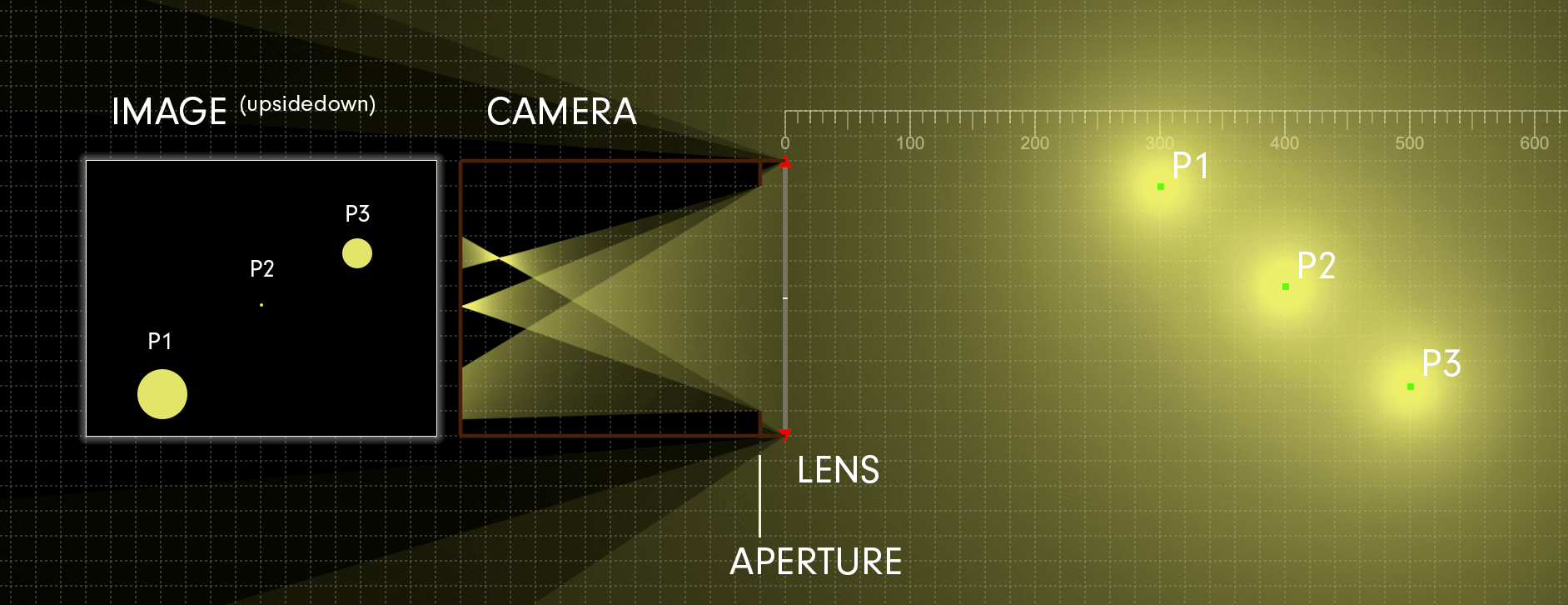
Light from any point in object space emerges from the rear element of a lens as a cone. When a subject point is in focus, the apex of its light cone coincides with the focal plane, which forms an image point in the photograph. If the subject point doesn’t come into perfect focus on the image sensor, it creates a small blurred circle called a circle of confusion. The three factors that control the depth of field—the aperture, focal length, and subject distance—do so by varying the size of the blur circles. The diameter of the circle of confusion with the resolution of the image sensor is used to calculate the depth of field.
The chemical composition of Optical Glass is designed to selectively transmit or block different wavelengths of light in the optical light spectrum, from UV Ultraviolet, to Visible light, to IR Infrared light. Valley Design laps, polishes , dices and CNC machines optical glass of all types, and works with the premier optical glass manufacturers such as Corning, Schott, and Hoya. Optical glass is used every day by consumers, for vision, magnification, telephotography, science research and more which is why precision and quality is key for optical glass suppliers such as Valley Design.
Subject distance. As the subject (on which you’re focused) moves progressively closer to the camera, the depth of field decreases.
depth offield中文
It’s important to understand that the depth of field is a theoretical calculation that doesn’t take into account lens aberrations, light diffraction, and post-capture manipulations such as sharpening and cropping.
Photographers exploit the depth of field all of the time to achieve effects such as deep or shallow focus. Deep focus photography relies on a considerable depth of field to achieve acceptable sharpness in the foreground, middle-ground, and background of the picture. This effect is often associated with landscape photography (where much of the image appears in sharp focus) and some forms of street photography. Shallow focus photography features a narrow or small depth of field, which is characterized by a sharply focused subject and an out of focus, or blurred, background and foreground. This technique is frequently used by portrait photographers—especially those working on location as opposed to in studio—because it visually separates the subject from the scene. Bokeh describes the aesthetic quality and character of how lenses render the out of focus elements in a picture.
Aluminum Nitride Ceramic is the perfect material choice when high thermal conductivity and electrical insulation properties are needed. Aluminum Nitride has a combination of high dielectric strengthening, high electrical insulation properties, and low thermal expansion. Valley Design supplies Aluminum Nitride with thermal conductivity of 170 W/mK, 180 W/mK, 200 W/mK and 230 W/mK. AlN Aluminum Nitride is optimal for hybrid, power and microwave electronics applications where an electrically insulating nontoxic substrate material is required. It is the ideal material for a wide variety of uses in the growing Semiconductor, Aerospace, Defense and Medical Industries.
An Optical Transmission Curve is a graph that shows an optical medium plotted against the wavelength. The graph describes the transmission fraction of an optical filter as a function of wavelength. These transmission curves can be used by optical designers and engineers to determine the most suitable material to use for their applications.
The depth of field is commonly expressed using units of length. The subject distance is measured from the focal plane of the camera (whose position is indicated on top of your camera with the focal plane indicator, ɸ) to the point in object space on which the lens is focused. The total depth of field is the entire range of acceptable focus. it’s measured from the near limit of acceptable focus, which lies between the camera and subject, and the far limit of acceptable focus, which lies between the subject and infinity.
There’s no truly objective measure for what qualifies as an acceptable degree of sharpness concerning the depth of field. A photograph that looks adequately sharp when enlarged to fit a 15-inch notebook display may appear slightly unsharp when expanded to a 30-inch desktop display. A 24×36 inch print may look sharp from across the room, less sharp from a comfortable reading distance, and downright blurry from the tip of your nose.
Valley Design laps, polishes and CNC machines a wide variety of metals and alloys including Stainless Steel, Aluminum, Copper, Hastalloy, Brass, Inconnel, Titanium, Steel Alloys, Low Carbon Steel, Tool Steel, Tungsten Carbide, Invar, Bronze, Kovar and Cast Iron Zinc. Mirror surface finishes as good as < 10 Angstroms are achievable on some metal materials.
Valley Design provides lapping and polishing services of flat mechanical seals, pump parts, valve seats and discs. Valve components made from a large variety of materials include Hastelloy, Inconel, Monel, Stainless Steel, Carbon Steel, Copper, Nickel, Ceramics, Glass, Sapphire, Macor and many exotic materials. We have even polished large wind tunnels for NASA.
Focal length. Lens focal length is a significant factor in managing the depth of field. Short focal length lenses produce greater depth of field, while long focal length lenses produce shallow depth of field.
In 1975, Valley Design began polishing 2” diameter Silicon wafers, then continually expanded our polishing capabilities in keeping with the Semiconductor Industry to 3” diameter, then 100mm, 125mm, 150mm, 200mm eventually landing at 300mm diameter. Looking forward, the Semiconductor industry contemplated transitioning lithography fabs to 450mm, but it was not generally accepted by the equipment manufacturers. Valley Design has performed back grinding and lapping of 450mm diameter Silicon wafers, and also routinely laps, polishes, dices and CNC machines Silicon in all sizes. Ultra-thin is also available as thin as 20um thick.
Depth of fieldgithub
Precision shims spacer and submount components from Valley Design with accurate pitch tolerances and sequentially spaced to less than 1/4 micron, flat to less than 1/10 wave, with lapped or polished mirror finishes available.
Valley Design produces and stocks wafers and substrates of Fused Silica and Fused Quartz as large as 300mm diameter to 1cm square to as thin as 10-15um thick. Advantages of Fused Silica and Fused Quartz include low thermal expansion, resistance to thermal shock, superior electrical insulation, high transparency from the Ultraviolet light spectrum to the Infrared range, high softening temperature and thermal resistance. Valley Design has thousands of finished Fused Silica wafers available from stock. Single Crystal Quartz is also available lapped, polished, diced and CNC machined.
In photography, space ahead of a lens is known as object space, while space behind is called the image space. In theory, rays of light from any point in object space should converge, or focus, at some point behind the lens. As the distance between the lens and subject changes, the distance behind the lens at which the subject is focused also changes. A subject farther from the camera will focus closer behind the lens than a nearby subject. [This is why macro lenses are capable of such a long extension: to bring very close objects into focus.]
CVD Silicon Carbide theoretically dense and intrinsically pure, is available as lapped or polished substrates and wafers from 2″ diameter up to 300mm diameter with surface finishes to better than 10 angstroms, while maintaining a 1/4 wave flatness depending on thickness and size.
Patented, our new non-contact interferometer, the Indars Interferometer, is designed to alleviate the problems inherent with using optical flats or Fizeau interferometers as discussed above. The Indars Interferometer has been specifically optimized for the flatness characterization of thin, transparent wafers, substrates and windows. Its unique design allows wafers to be positioned vertically, eliminating most bending forces applied by gravity and without necessitating the application of flatness distorting films.
Depth of fieldcalculator
Valley Design produces standard and custom lapped or polished Sapphire wafers in all common orientations including A, C and R-plane Sapphire. Valley also provides ultra-thin polished Sapphire substrates and wafers. The size of Sapphire that can be polished is limited only by the material availability. Sapphire blanks up to 12″ diameter can be lapped, optically polished, diced and CNC machined. Holding precise tolerances as well as flatness, and parallelism is critical for many applications.
Valley Design manufactures wafers, substrates and discs from all materials including Fused Silica, Glass of all types, Colored Filter Glass 96% Alumina, 99.6% Alumina and Aluminum Nitride ceramics, Sapphire, CVD Silicon Carbide SiC and metals including Stainless Steel. We provide wafers in SEMI standard sizes, as well as custom sizes, and have 1,000’s of finished wafers and substrates available from stock.
Valley Design proudly offers special capabilities to our CNC machining services such as ultra thinning to as thin as 10-15um, polishing to Angstrom level finishes, micron level tolerances and TTV (Total Thickness Variation) specifications. We process a wide variety of materials from our extensive inventory, as well as customer supplied materials. Commonly processed materials include ceramics of all types, 96% Alumina, 99.6% Alumina, Aluminum Nitride, Fused Silica, Glass, Sapphire, Macor, Silicon Carbide SiC, Silicon Silicon-Carbide SiSiC and many others.
At Valley Design, we are the experts in precision dicing. Our dicing services can cover all your needs from prototypes to production dicing services. With 15 K&S and DISCO dicing saws, we have one of the highest diamond dicing volume capacity in the industry. Silicon die from as small as .127mm square to Silicon stacks as high as 6.25mm can be diced, as well as a wide variety of hard materials including Fused Silica, Glass, Aluminum Nitride, Alumina ceramics, Sapphire, Silicon Carbide SiC, Silicon Silicon-Carbide (SiSiC) and many others.
Depth of field
Valley Design serves numerous high-tech industries including Semiconductor, Medical and Biomedical, Aerospace, Defense and Sensing, Photonics and Optics, Telecommunications, Lithography, along with Research and Development industries. Applications include Substrates, Wafers and Electro-optical and Micro-electronic components for sensors, integrated circuits, capacitors, semiconductors, optoelectronics, microfluidics, MEMS devices, Machine vision, Optical Switches, Electro static chucks (ESD) for ion implanters, and optical instrumentation.
Precision lapping and polishing services on all types of materials both hard and soft has been a specialty of Valley Design for nearly 50 years. We operate over 100 single and double sided lapping and polishing machines ranging in size from 12”,18”,24” 28”, 32” 36”48”and 64” diameters producing parts from as small as .127mm (.005”) sq. to 450mm diameter and larger. Depending on the material, lapped finishes can range from 10-25u” Ra. Polished surfaces on ceramics can range from 0.3 -3u” Ra, and optical finishes on fused silica and glass can be as good as 3A Ra.
Shallowdepth of field
Measuring flatness using an optical flat entails direct contact between the specimen to be measured and the optical flat itself. Holding the surface of a high precision optical flat against the test specimen under monochromatic light creates visible light bands, which are formed by the air gaps where the two surfaces are not in perfect contact. These interference fringes show the contour of the surface under test. The light and dark patterns visually represent the flatness of the surface being tested, and it is the curve and spacing between these fringes which indicate the surface accuracy.
Valley Design offers a wide variety of optically polished metal mirrors including Stainless Steel, Molybdenum, Brass, Copper and many other alloys. Surface roughness of < 10 Angstroms are possible on some materials. Metal chucks and vacuum chucks are lapped, polished and CNC machined to micron level tolerances.
Email: info@valleydesign.com Phone: 978.425.3030 Fax: 978.425.3031
As a leader in precision materials processing for nearly 50 years, Valley has extensive experience with a wide variety of materials. We process various semiconductor materials, optical materials and materials used in electro optics.


 Ms.Cici
 8618319014500