
Bar Lights - lights for outdoor bar
Flying probe testing is a tried-and-true option that’s less expensive than in-circuit testing. It’s a nonpowered type of test that checks for:
X-ray testing can check elements that are usually hidden from view, such as connections and ball grid array packages with solder joints underneath the chip package. While this check can be very useful, it does require trained, experienced operators.
PCB visualinspectionprocedure

AOI can be useful for detecting issues early to ensure production is shut down ASAP. However, it does not power up the board and may not have 100% coverage for all part types.
Here’s a primer on the most important types of PCB testing. This should prepare you better for discussions with your ECM:
PCBinspectionstandard
This test involves using fixed probes laid out in a way that matches the design of the PCB. The probes checks the integrity of the solder connection. The bed of nails tester simply pushes the board down on the bed of probes to start the test. There are access points predesigned in the board that allows the ICT testing probes to make connections with the circuit. They put a certain amount of pressure on the connection to make sure it stays intact.
Never rely solely on an automated optical inspection. AOI should be used in conjunction with another test. Some of our favorite combos are:
In some cases, ICT makes it unnecessary to use flying probe testing, but the PCB has to be designed to fit with the test fixture -- which means a higher initial cost. ICT can be faster and less error-prone than flying probe testing, so you might find the extra cost is worth it. While flying probe testing can be cheaper initially, it may actually be less cost-effective for large orders.
There are customers who do like a good, old-fashioned functional test. Your ECM uses this to verify that the product will power up.
PCB manual visualinspection
Also, note that your ECM can’t necessarily inspect every layer of a board using an X-ray machine. It’s true we can see through the board to detect internal defects, but it’s a very time-consuming and expensive process (for both ECM and customers).
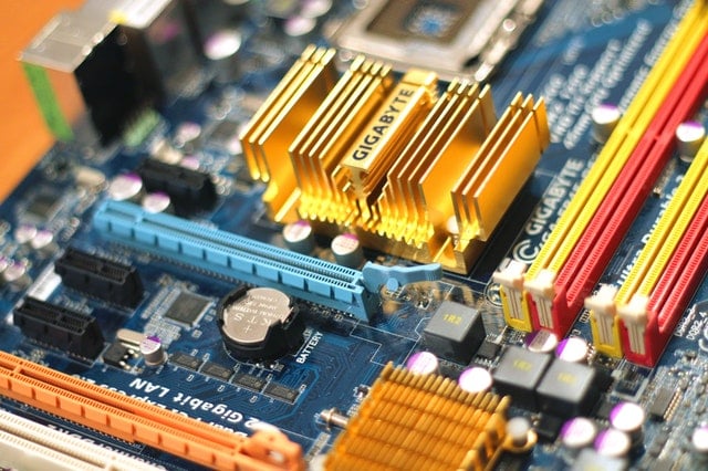
When you order printed circuit boards (PCB), you know the pricey consequence of failure. The last thing you need financially is for your PCBs to suddenly drop dead -- or to have a shortened life span because of a design or QA issue.
[4] On the mixed critical response to Saarinen’s work, see Friedman, American Glamor, 112-14, and Vincent Scully, “Rethinking Saarinen,” in Eero Saarinen: Shaping the Future, Eeva-Liisa Pelkonen and Donald Albrecht, eds. (New Haven: Yale University Press), 13-14.
PCB assembly testing methods are an integral part of the manufacturing process. Reputable electronics contract manufacturers (ECMs) offer a variety of PCB testing methods, but the seven main types include:
An ICT, also known as a bed-of-nails test, powers up and actuates the individual circuitry on the board. In most cases, the test is designed for 100% coverage, but you’ll get closer to 85-90% coverage. The nice thing about ICT is that the 85-90% you get is totally free of human error.
The flying probe tester works through the use of needles attached to a probe on an x-y grid obtained from basic CAD. Your ECM programs coordinates to match the circuit board and then runs the program, connected to those test points.
A PCB functional test verifies a PCB’s behavior in the product’s end-use environment. The requirements of a functional test, its development, and procedures can vary greatly by PCB and end product.
While the Technical Center is also associated with a number of other nationally significant individuals, including automobile and industrial designer Harley Earl and General Motors executives Alfred P. Sloan and Charles F. Kettering, the Technical Center illustrates neither the areas of significance of these individuals nor, more importantly, the period in which the nationally significant achievements of these men were made. Further, while the nationally significant landscape architect Thomas Church was involved in the design of the Technical Center, it cannot be considered to be a signature design by Church. In contrast to the domestic projects for which Church is most widely known and recognized, and on which he himself wrote influentially for a large American audience, Church contributed aspects of the landscape to the Technical Center, but was not the design leader for it. The project is undoubtedly characterized by a degree of technical and artistic collaboration, but under the principal design aegis and direction of Eero Saarinen.
(Editor's Note: This article was originally published in September 2019 and was updated in May 2024 to reflect up-to-date and current information.)
Burn-in testing pushes power through your electronics, usually at its maximum-specified capacity. The power is run through the board continuously for 48 to 168 hours. If a board fails, it is known as an infant mortality. For military or medical applications, boards with high infant mortality are clearly not ideal.
PCB design is tricky. Depending on how complex your project is — or how much is at stake if something fails — you may need top-end testing before...
In-circuit testing (ICT) is the most robust type of PCB testing in existence. The high price reflects that -- tens of thousands of dollars, though the cost will depend on board and fixture size, among other factors.
PCBinspectionmethods

Figuring out what PCB testing is right for you can be a challenge; there are certainly a lot of methods! Your ECM will know which tests are right for your specific needs, so consult with them often.
And don’t forget about PCB prototyping. This essential element of product launches acts as a test in its own right, allowing you to see the real thing before your market does.
This functional test and its parameters are usually provided by the customer. Some ECMs can help develop and design such a test.
Just remember that burn-in testing can shorten the product’s lifespan, especially if the test puts your board under more stress than it’s rated for. If few or no defects are found, it's possible to reduce the testing limit after a shorter period to avoid over-stressing your PCBs.
For more detailed information on PCB testing and prototyping, and even first article inspections, download this free e-book:
PCB visualinspectionchecklist
AOI uses either a single 2D camera or two 3D cameras to take photos of the PCB. The program then compares the photos of your board to a detailed schematic. If there is a board that does not match the schematic to a certain degree, the board is flagged for inspection by a technician.
As a number of authors have noted, Saarinen’s collaborative approach with his clients was a key to the success of his projects with them: as Friedman puts it – “communicating the identity and meaning of the individual project,” by taking his cues from the corporate culture and identity of his clients.[2] This collaborative method and tendency to vary his approach to style to express the nature of the project and the client, as opposed to the autocratic imposition of form in a project, was one that would later lead to mixed critical reception for Saarinen, although the reception of the Technical Center itself was almost universally laudatory. As his widow Aline remarked after the architect had died, “the critics punished him often.” The architect Robert Venturi, who worked in the Saarinen office during the Technical Center project, encapsulated one key aspect of the objections to his methods in a critique of the firm soon after he left it, saying that Saarinen “did not have a singular approach,” which Venturi took “as a sign of weakness.”[3] Saarinen’s approach to clients such as GM was seen as pandering by some: for example, Manfredo Tafuri, the noted Italian architect, historian, theoretician and critic, derided Saarinen’s approach as “corporate advertising” and the influential historian, author, and Yale University professor Vincent Scully was at best lukewarm about Saarinen’s approach, believing that Louis I. Kahn and Robert Venturi “offered a much better way toward a reasonable future for architecture” than Saarinen’s more eclectic strategy did. [4] Despite this divided critical response to Saarinen’s corporate work in his lifetime, the architect’s collaborative and expressive method unquestionably made the architect one of, if not the most important designer in the American public imagination in the period: he was the architect who both captured and enormously influenced the post-war culture. The Technical Center was the project that created Saarinen’s broad American stature and working method, and was deeply rooted in GM’s own culture. In essence, it made Saarinen famous. It also caused his office to grow from a small staff to one of forty people, many of whom, including Gunnar Birkerts, Kevin Roche, John Dinkeloo, Cesar Pelli, Anthony Lumsden, Joseph Lacy, J. Henderson Barr, Olav Hammerström, and Venturi, went on to have extremely important careers as modernists. The Technical Center established Eero’s identity as an independent, world class designer in his own right. It thus took his career beyond its early phase of its association with his father – in which Eero always stood to a certain extent in Eliel’s shadow – to a nationally significant career ended prematurely in 1961.
This test is for a “mature” product with very few revisions expected. If you don’t have design-for-manufacturing as part of your goal, with the proper pads on the board, you may not be able to use an in-circuit test. Unfortunately, you can’t change your mind and move to an ICT strategy halfway through production.
[1] Alice Friedman, American Glamor and the Evolution of Modern Architecture (New Haven: Yale University Press, 2010), 109.
People: Florence Knoll , Kevin Roche , Smith, Hinchman & Grylls , Peter Petkoff , Eero Saarinen , ,
PCBinspectionmachine
Burn-in testing isn’t for every project, but there are some cases where it makes a lot of sense. It can prevent embarrassing or dangerous product launches before they reach customers.
Architectural historian Alice Friedman has noted in her recent American Glamor and the Evolution of Modern Architecture that, in his career cut short by his sudden death from a brain tumor in 1961, Eero Saarinen achieved an astounding amount of national success in his practice. As she further remarks, this success rested on a series of “corporate headquarters and campus-like research centers for many of the household names of American industry and manufacturing” as well as “plum government jobs.” Friedman accurately notes that these projects “put a very public stamp of approval on Saarinen’s distinctive approach to architecture, handing him the lion’s share of responsibility for creating a new American style for the postwar age.”[1] In contrast to other architects revered by their peers but relatively unknown to the American public, Saarinen’s acclaim reached a broad audience through these projects. This acclaim was established by the General Motors Technical Center, which marked the point when Saarinen’s career diverged from his collaboration with his father Eliel Saarinen. Eero had been leading certain design projects within the firm of Saarinen, Swanson and Saarinen before the Technical Center, and had been engaged in such important independent endeavors as his experiments in chair, structure, and house design with Charles Eames of the late 1930s and early 1940s, but his practice remained essentially subsidiary to Eliel’s until the father’s death in 1950. The Technical Center project allowed Eero’s practice not merely to survive his father’s death, but also to grow significantly beyond it, establishing a highly public, separate, independent identity. This identity was one that was recognized much more broadly than Eliel’s own substantial professional reputation, beginning with, and thanks to the Technical Center project, along with the Jefferson Memorial project, which was begun at the same time.
Your great, new electronics product is almost ready to go. All you need is ICT testing (in-circuit testing) -- or perhaps another method of testing.
It does take time. If you want to get your product out the door quickly, this may not be your best choice. But from a quality and longevity standpoint, functional testing can save face and save money.
The General Motors Technical Center is nationally significant as one of the most important works of architect Eero Saarinen (1910-1961). The Technical Center represents several key aspects of this renowned architect’s career. The first of these is that the Technical Center marks his emergence onto the international stage as an important designer independent of his work with his father Eliel, first bringing him to wide national attention and acclaim. The Technical Center project was embraced around the world as the embodiment of the spirit of the post-World War II age in America and of the prosperity and modernity of the nation and its people. The second of these is that this campus represents Saarinen’s work not just as a creator of buildings, but as the planner/designer of total environments. At the Technical Center, Saarinen worked with and orchestrated key collaborators on the campus’s buildings and their material details, construction methods, landscape, furniture and furnishings, and artwork, creating a design totality unparalleled in the period that established a key working method for the architect. Finally, the Technical Center is also significant as the first of four influential Saarinen suburban corporate campuses (along with later projects for IBM, Bell Laboratories, and John Deere), that set the design standard for this important post-World War II landscape and architectural type that represented a sea change in American business facilities.
Electronics manufacture and testing are like squabbling siblings. PCB testing is a necessary expense that, when done correctly, prevents much larger...
As the name suggests, burn-in testing is a more intense type of testing for PCBs. It’s designed to detect early failures and establish load capacity. Because of its intensity, burn-in testing can be destructive to the parts being tested.


 Ms.Cici
 8618319014500