
Optical Tool 3.0 - eyeglass lens thickness calculator
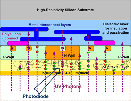
Then the backside of the sensor wafer is optionally thinned and an optionally anti-reflective coating is applied and the sensor is mounted upside down. Then the photocathode well is directly exposed to photo-electrons and no photo-electrons are thus blocked by the associated overlying electronics. This and lateral capture results in significantly increased quantum efficiency.
BSI CMOS
Optical format
The F-number is only defined for objects at infinite distance. The sensor has according the definition of the focal length exactly the distance “focal loength” from the principal plane when the lens is focussed to infinity.
where working F-number or effective F-number. image side numerical apertur, the magnification for this focus distance and is the pupil magnification.
Alacron, Inc. is capable of processing sensor wafers to produce backside illuminated wafers or sensors on a contract basis. Backside illumination is performed to allow the sensor to be illuminated on the side opposite the electronics of the sensor.resulting in significantly increased quantum efficiency. This allows increased light sensitivity or reduced pixel pitch.
Back sideilluminated
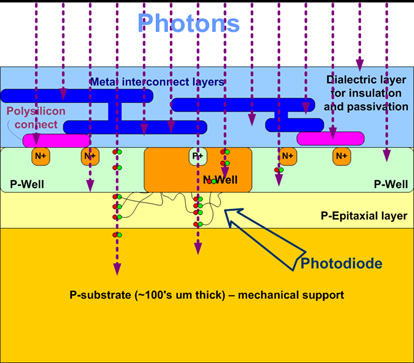
A typical image sensor such as the CMOS sensor pictured below has the electronics layers overlaying part of the pixel area. Photons entering the sensor are thus blocked by the structures overlying the photocathode as well as the associated electronics in the pixel well. This results in the reduction of photon conversion efficiency with the resultant decrease in quantum efficiency.
To keep the object focussed, the distance of lens and sensor must be increased. This is equivalent with adding distance rings reagrding the infinity position of the lens. As result the images gets darker the field of view gets smaller , the therefore the magnification changes.


 Ms.Cici
 8618319014500