
Macro Lenses - lenses macro
Customers building next-generation camera sensor products for various applications may rely on Camera Image Processing to provide the best solutions.
The image sensor in a camera system receives incident light, or photons, that have been focused by means of a lens or other optics.
Users can select a number between 1 and 1000 to have their signal multiplied that many times in the EM Gain register as part of this step-by-step EM process.
The incident light (photons) is focused by a lens or other optics and is received by the image sensor in a camera system.
Camera sensor
Understanding CMOS imagesensor
On a sensor, electrons can be carried in any direction in this way, and they are often moved to a location where they can be amplified and turned into a digital signal, which can then be presented as an image.
To deliver a high-quality image for a specific camera sensor and use case, an ISP could carry out several procedures, including black level reduction, noise reduction, AWB, tone mapping, color interpolation, autofocus, etc.
Therefore, in addition to having a lot of pixels, factors like drive technology, quantum efficiency, and pixel size structure all impact imaging performance in different ways.
It is divided into four categories, such as contact image sensor (CIS), charge-coupled device (CCD) image sensor, front side illuminated (FSI), backside illuminated (BSI), and complementary metal oxide semiconductor (CMOS) image sensor.
The basis for how digital cameras take and create images is thus the camera sensor, which is essential in transforming light into digital information that can be further processed and saved.
CMOSsensor
EMCCDs provide quicker and more sensitive imaging than CCDs, making them ideal for photon counting or low-light imaging devices.
As CMOS sensors have a far lower read noise than CCD/EMCCD, they can work with weak fluorescence or live cells and move electrons much slower than the projected maximum speed.
The market for complementary metal-oxide semiconductors, or CMOS and sCMOS image sensors, has grown significantly in recent years.
LED Commercial Lighting · Utilitech. 4-ft 4000-Lumen White Cool White LED Flush Mount Garage Shop Light · Lithonia Lighting. 4-ft 2900-Lumen Cool White LED ...
This technology’s lack of sensitivity and speed constrained the number of samples that could be scanned at acceptable levels.
Due to its ability to be multiplied up above the noise floor as many times as needed, EMCCDs can now detect tiny signals.
When an EMCCD receives a signal of 5 electrons, and the EM Gain is set to 200, the output node will receive a signal of 1000 electrons.
Due to inadequate illumination and other environmental factors, the captured image may contain some unnecessary elements despite each specific sensor, processor, and lens combination.
Temporary Storage: Processed photos may be stored in the camera’s buffer (6) indefinitely while they wait to be written to the memory card.
Signal Conversion: An electrical signal that could be weak is produced by the sensor. Analog electronics (3) increase this signal by amplifying it.
3D Imaging: There are now more uses for CMOS image sensors in augmented reality, industrial inspection, and healthcare thanks to their development of 3D imaging capabilities.
Große Auswahl neuer und gebrauchter Pc Gehäuse Beleuchtung online entdecken bei eBay.
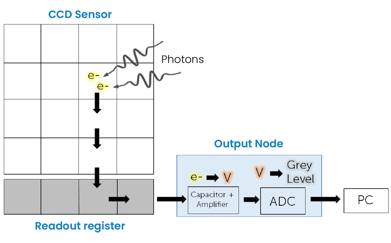
The transformation of light photons into electrons is the first process for a sensor (known as photoelectrons). Quantum efficiency (QE), which is displayed as a percentage, is the efficiency of this conversion.
According to Skyquestt, With a projected size of USD 16.25 billion in 2019 and a projected growth rate of 9.6% during the forecast period (2024–2031), the image sensor market is expected to reach USD 39 billion by 2031 from USD 16.36 billion in 2023.
This was accomplished in several ways via EMCCDs. The cameras’ back illumination (which raises the QE to over 90%) and massive pixels (16-24 m) significantly raise their sensitivity.
Wir bieten für jedes Event die richtige Location. Plane deine Veranstaltung in Frankfurt (Oder) | Kleist Forum | Konzerthalle | Messehallen.
CMOS sensors use an on-chip analog-to-digital converter (ADC) to transform photons into electrons, voltage, and finally a digital value.
The development and spread of consumer electronics with imaging capabilities underscore the increasing importance of camera image processing.
Because the speed at which electrons are moved around a sensor increases read noise, CCDs move electrons much slower than their maximum potential speed.
Le ottiche a fuoco fisso sono inoltre ideali per le applicazioni di visione in quanto i pezzi vengono solitamente presentati alla telecamera in una posizione ...
There are two major types of image sensors: CCD, or charge-coupled device, and CMOS, or complementary metal oxide semiconductor.
Electrons go from the image array to the masked array, and then onto the readout register in a manner that is remarkably similar to frame-transfer CCDs.
This implies that positive voltages can attract electrons, making it possible to move electrons across a sensor by applying a voltage to particular sensor regions.
Compared to CCD/EMCCD technology, this combination enables CMOS sensors to operate parallel and analyze data more quickly.
Camera sensorstructure
The current generation of intelligent devices, which represent a quantum jump in sophistication, is made possible by camera competence.
According to datahorizzonresearch, the market growth of CMOS and sCMOS image sensor market size was valued at USD 23.3 Billion in 2023 and is expected to reach a market size of USD 40.8 Billion by 2032 at a CAGR of 6.4%.
All electrons have a negative charge that underlies the operation of all the sensor types covered here (the electron symbol being e-).
An image signal processor (ISP) is a processor that receives a raw image from the image sensor and outputs a processed version of that picture (or some data associated with it).
To evaluate the camera sensors’ tuning, image quality, and image resolution, various types of labs tools are required, such as;
For example, if a CCD detects a signal of 10 electrons with a read noise of 5 electrons, the signal could be read out at any value between 5 and 15 electrons, depending on the read noise.
Additionally, each ADC has to read out considerably less data than a CCD/EMCCD ADC, which must read out the complete sensor because there is an ADC for every column.
While CCD and EMCCD technologies were popular for scientific imaging, sCMOS technology has emerged in recent years as the best option for imaging in the biological sciences.
Serie I Nostri Banchi. I banchi tecnici I Nostri Banchi sono espositori per piastrelle che si integrano in zone tecniche di lavoro. Scopri tutti i moduli che ...
Nowadays, charge-coupled devices(CCD camera sensors) and complementary metal oxide semiconductor technology (CMOS) imagers make up the majority of sensors.
These neural networks will be able to detect suspicious behavior and transmit an alarm in real time, instead of depending just on motion detection.
2020419 — A camera sensor and its size determines image size, depth of field, resolution, low-light performance, a camera's physical size, and more.
2021726 — 16.1 mm. Depth (inches). 0.634 inch. Height. 18.86 mm. Height (inches). 0.743 inch. Width. 29.9 mm. Width (inches). 1.177 inch. Net weight. 3.94 ...
EMCCD Fundamentals – Camera Sensor TechnologiesThe above image explains, How an EMCCD sensor works. Photons hit a pixel and are converted to electrons, which are then shuttled down the sensor integration to the readout register.
The sensor collects light and transforms it into an electrical signal that is subsequently processed to create a digital image, much like the retina in a human eye does the same thing by translating light into nerve impulses that the brain can understand.
Main > Product > Machine Vision Area Scan camera > Allied Vision Industrial Machine Vision Cameras ; Allied Vision, Alvium 1800 U-040C, USB3, IMX287, CMOS Global ...
Obtaining the ideal image or video quality is tricky for each use scenario. A lot of filtering and iterations are necessary to attain a desirable outcome.
The image processing sector is currently one of the global businesses with the fastest growth rates, and as a result, it is a crucial area of engineering study.
Moreover, barcode readers, astronomical telescopes, and scanners all use these electronic chips. Low-cost consumer gadgets are possible thanks to CMOS’s inexpensive manufacture.
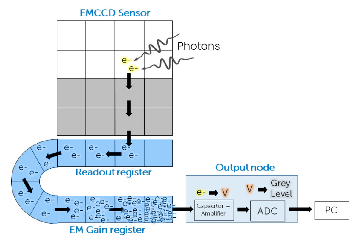
EMCCDs are far more sensitive than CCDs thanks to the combination of large pixels, back illumination, and electron multiplication.
The images are processed by imaging software on this node, amplified to readable voltage, and transformed into digital grey levels using an ADC.
After being exposed to light and changing from photons to photoelectrons in a CCD, the electrons are transported down the sensor row by row until they reach the readout register, which is not exposed to light.
Digital Conversion: After being amplified, the signal is passed to an analog-to-digital converter (4), which changes it into digital data that the camera can process more easily.
Image Processing: The digital data is routed to the image processor (5), where it is subjected to several enhancements and modifications, including sharpening and color correction.
Machine vision covers flat panel displays, PCBs, semiconductors, warehouse logistics, transportation systems, crop monitoring, and digital pathology.
Photons hit a pixel, converting to electrons that move to the sensor’s readout register, then to the output node where they become voltage, then grey levels, and finally displayed on a PC.
The choice of the appropriate camera sensor has become extremely important and varies from product to product because cameras have a wide variety of uses in many industries.
A full-frame CCD sensor is a kind shown in Figure 2, although there are also additional designs known as frame-transfer CCD and interline-transfer CCD.
The EM Gain register now becomes the primary point of distinction. Impact ionization is a technique EMCCDs to drive more electrons out of the silicon sensor size, doubling the signal.
The primary purpose of these sensors is to produce images for digital cameras, digital video cameras, and digital CCTV cameras.
Light entering a digital camera through the lens hits an image sensor. The camera processes the signal that the image sensor outputs to produce image data, which is then saved on the memory card.
The sensor’s ability to transmit data as either a voltage or a digital signal to the following stage will depend on whether it is CCD or CMOS.
Optical imaging systems often generate panchromatic, multispectral, and hyperspectral imagery using visible, near-infrared, and shortwave infrared spectrums.
An integrated circuit that is sensitive to light and uses photons and electrons to create images is called a charge-coupled device, or CCD. Pixels are separated from the image elements using a CCD sensor.
Camera Sensor integration, image sensor integration, and camera image processing methods are widely utilized in various applications
They are amplified using the EM Gain register, sent to the output node, converted to a voltage, grey levels, and then displayed with a PC.
These electrons can be moved pixel by pixel anywhere on a sensor by employing a positive voltage (orange) to transfer them to another pixel.
Ich würde mich sehr über Angaben weiterer interessanter Quellen freuen!!Hinweis: Alle Angaben über Wasser sind nach bestem Wissen gemacht worden, jedoch ist jeder selbst verantwortlich, jegliches Wasser aus Brunnen und Quellen zu trinken!!!
For sensitive, quick imaging of a range of samples for several applications, quantitative scientific cameras are essential. Since the invention of the first cameras, camera technology has developed significantly.
The information transferred to the following stage by the sensor will be either a voltage or a digital signal, depending on whether it is a CCD or CMOS sensor.
High-Resolution Sensors: There is a growing trend towards higher resolution CMOS image sensors, enabling sharper and more detailed images.
The behavior of the readout electronics serves as the integration’s boundary, which is unrelated to the shutter’s exposure.
Photons hit a pixel, are converted to electrons, and then to the voltage on the pixel. Each column is read out separately by individual ADCs and then displayed with a PC.
CCD sensor Works – Camera Sensor TechnologiesThe above image explains the Different types of CCD sensors. The full-frame sensor is also displayed. Grey areas are masked and not exposed to light.
Nikon Fx Format Lenses(266) · Nikon AF-S DX NIKKOR 35mm f/1.8G Lens · Nikon AF-S Nikkor 50mm f/1.8G Fixed Focal Length Lens · Nikon Z 35mm f/1.4 Lens, 62 (Jul 18th).
Every pixel is transformed into an electrical charge, the strength of which is correlated with the amount of light it was able to collect.
10"Inch Led Ring Light with Tripod Stand For Tiktok|Youtube|Reels|Photo-shot|Video Live stream| Makeup Videos|Vigo Video Shooting|3 Color Modes |Dimmble ...
The sensor collects light and transforms it into an electrical signal that is subsequently processed to create a digital image, much like the retina in a human eye does the same thing by translating light into nerve impulses that the brain can understand.
The growth behind these image sensors is due to the growing need for high-performance, low-power, and reasonably priced imaging solutions across a range of industries.
A sensor transforms a physical event into a quantifiable analog voltage, or occasionally a digital signal, which is then sent for reading or additional processing or transformed into a display that is readable by humans.
Sensorformat
The frame-transfer sensor has an active image array (white) and a masked storage array (grey), while the interline-transfer sensor has a portion of each pixel masked (grey).
Without the container, an integrated sensor is only the sensor’s fundamental technology. It enables various sensor technologies to be “integrated” or combined into a single plug-and-play component.
This includes camera integration, camera image processing, CMOS image sensor technology tuning, and other related capabilities.
AI Transforming Photography: Camera technology is being revolutionized by AI and machine learning, with possible uses ranging from improving image authenticity to countering bogus AI-generated photos.
From consumer to computer vision to industrial, defense, multimedia, sensor networks, surveillance, automotive, and astronomy.
This implies that the pixel converts a photon into an electron and that the electron is then instantly changed into a readable voltage while still on the pixel.
A pixel (blue squares) is struck by photons (black arrows), which are then transformed into electrons (e-), which are then stored in a pixel well (yellow).
By selecting the best camera manufacturer technology for your imaging system, you can enhance all aspects of your studies and conduct quantitative research.
CMOS sensor technology allows for greater speeds due to its parallel operation, unlike CCD and EMCCD which rely on different methods of sequential operation.


 Ms.Cici
 8618319014500