
Overview of Laser Types and Lasing Media - types of laser light
After the images of the circuits are recorded in the photoresist film, etching tools are used to transfer those circuit patterns into the silicon wafer, eventually forming hundreds of computer chips on each 12-inch wafer.
The angle between the output polarization and the input polarization will be twice the angle between the input polarization and the wave plate’s axis (see diagram to the lower right). When the polarization of the input beam is directed along one of the axes of the wave plate, the polarization direction will remain unchanged.
Advances in microelectronics – also known as microchips or chips – have enabled fast, powerful, compact smartphones and laptops – electronic devices that were once, long ago, the stuff of science fiction.
Advancing microelectronics is a strategic R&D direction for Berkeley Lab, and the CXRO’s activities over the last 25 years are a major component to that. In addition to collaborating with the semiconducting industry to extend Moore’s Law, CXRO researchers are also helping other Berkeley Lab scientists develop next-generation chips that are also more energy efficient than conventional silicon chips.
A quarter-wave plate is designed such that the phase shift created between the fast and slow axes is a quarter wavelength (λ/4). If the input beam is linearly polarized with the polarization plane aligned at 45° to the wave plate's fast or slow axis, then the output beam will be circularly polarized (see image at right). If the linearly polarized beam is aligned at an angle other than 45°, then the output will be elliptically polarized. Conversely, the application of a circularly polarized beam to a λ/4 wave plate results in a linearly polarized output beam. Quarter wave plates are used in Optical Isolators, optical pumps, and EO Modulators.
Quarter-WaveplateThorlabs
In 2001, as EUV lithography gained more traction across the industry as a whole, we kicked off a partnership with SEMATECH, which was a broad-based semiconductor industry consortium, to continue pushing EUV lithography research forward.
Half-waveplateJones matrix
Q: What is the CXRO doing now to push chip innovation forward? During the pandemic, we continued to partner with Intel and Samsung to push the capabilities of our next generation EUV lithography research tools and to develop new chemical analysis tools that allow us to understand the fundamental physics of how photoresists work.
Q: How has CXRO helped drive innovation in chip making? The CXRO has helped industry understand the fundamental science behind EUVL, and how to push the technology forward.
The photoresist-coated wafer is loaded into the lithography tool and projected with tiny circuits using an EUV light. (Credit: Marilyn Sargent/Berkeley Lab)
In 1997, Intel, IBM, AMD, and Motorola formed the EUV LLC consortium to fund work at three national labs – Berkeley Lab, Livermore Lab, and Sandia – to develop the world’s first EUV lithography scanner for the semiconductor industry. I had just completed my Ph.D. when I was recruited by CXRO to work on the project. I’m proud to say that our work helped lay the foundation for the full commercialization of EUV lithography, which finally happened in 2019.
Half-waveplate
Achromatic Wave Plates provide phase retardance that is relatively independent of wavelength over a wide spectral range, and Superachromatic Wave Plates provide phase retardance almost entirely independent of wavelength over a much wider range than achromatic wave plates. In contrast, zero-order and multi-order wave plates provide a phase shift that is strongly wavelength dependent. Our achromatic wave plates are available with four operating ranges: 260 - 410 nm, 350 - 850 nm, 400 - 800 nm, 690 - 1200 nm, and 1100 - 2000 nm. Additionally, we offer superachromatic wave plates for the 310 - 1100 nm and 600 - 2700 nm ranges.
According to Naulleau, the tiny wavelength in EUVL is very close to X-ray light and therefore requires new instruments that far exceed the capabilities of early lithography, which employed longer and less energetic wavelengths of visible and ultraviolet light. (On the electromagnetic spectrum, a system scientists use to classify all ranges of light according to their corresponding wavelength, X-ray light ranges from 0.01 to 10 nanometers; extreme ultraviolet or EUV light ranges from 10 to 124 nanometers; and UV light from 124 to 400 nanometers, Naulleau explains.)
What does a half-waveplatedo
Multi-Order Wave Plates are made such that the retardance of a light path will undergo a certain number of full wavelength shifts (also referred to as the order, or m) in addition to the fractional design retardance. Compared to their zero-order counterparts, the retardance of multi-order wave plates is more sensitive to wavelength and temperature changes. Multi-order wave plates are, however, a more economical solution for many applications where increased sensitivities are not an issue. Our multi-order wave plates are available for a number of discrete wavelengths ranging from 405 nm to 1550 nm. Thorlabs also offers Dual-Wavelength Multi-Order Wave Plates designed for use at both 532 nm and 1064 nm.
That’s our value add – we do the fundamental research needed to accelerate technology a decade ahead of the game because the microchip industry doesn’t have time to wait.
Since the 1960s, the chip industry has relied on lithography – a technique that uses light to print tiny patterns on silicon to mass produce microchips. Through the decades, advances in lithography have enabled the use of smaller and smaller wavelengths and thus fabricate smaller transistors. During the early years of chip innovation, lithography tools once used visible light, with wavelengths as small as 400 nanometers (nm), and then ultraviolet light (as small as 248 nm) and deep ultraviolet light (193 nm).
We’re one of the first DOE labs to develop the basic research for EUVL systems – so industry relies on us to develop new EUV research and development instrumentation such as advanced microfield lithography and microscopy tools.
Zero-order wave plates are designed such that the phase shift created is exactly one quarter or one half of a wave. They offer substantially lower dependence on temperature and wavelength than multi-order wave plates. Our Zero-Order Quartz Half-Wave and Quarter-Wave Plates are composed of two wave plates stacked together with the fast axis of one aligned to the slow axis of the other to achieve zero-order performance. Thorlabs' zero-order wave plates are available for a number of discrete wavelengths ranging from 266 nm to 2020 nm. Our Polymer Zero-Order Half-Wave and Quarter-Wave Plates consist of a thin layer of liquid crystal polymer retarding material sandwiched between two glass plates and are available at discrete wavelengths between 405 nm and 2700 nm. Our quartz zero-order wave plates provide better retardance accuracy and lower reflectance (see table), while our LCP zero-order wave plates produce a smaller decrease in retardance at larger AOIs. In addition, Thorlabs also offers unmounted true Zero-Order Telecom Wave Plates for WDM applications.
EUV lithography was recently commercialized in 2019, but it took decades of research to get there, much of which was made possible by the unique capabilities of the CXRO. For the past 25 years, CXRO scientists and engineers have worked side by side with microelectronics industry leaders to tackle the significant technological advances required to develop EUVL.
Full waveplate
Q: How is EUV lithography used to make microchips? Naulleau:First, a photoresist is spread on top of a silicon wafer. A photoresist is a light-sensitive chemical film like we used to use in old-school film cameras.
DOE’s Office of Science is the single largest supporter of basic research in the physical sciences in the United States, and is working to address some of the most pressing challenges of our time. For more information, please visit energy.gov/science.
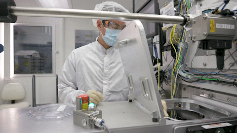
Researchers check the wafer after etching tools transfer circuit patterns onto the surface. (Credit: Marilyn Sargent/Berkeley Lab)
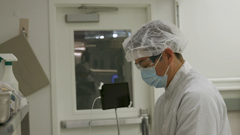
In this clean room at Berkeley Lab’s Center for X-Ray Optics, researchers use extreme ultraviolet lithography (EUVL) to advance the creation of next-generation, ultra-small computer chips. A human hair is 50–100 micrometers. Each image from the EUVL system is 200 x 30 micrometers and is extremely information-rich.
Quarterwaveplateformula
In addition to these options, Thorlabs also has the ability to design and manufacture custom wave plates for both OEM sales and individual low quantity orders. Our technical staff is able to help with all phases of your request: quoting, sales, and planning and manufacturing support. If you have a custom request or a question about our capabilities, please contact Tech Support to start a discussion.
Thorlabs offers achromatic, superachromatic, zero-order (both unmounted wave plates and mounted wave plates), low-order, and multi-order wave plates (single wavelength and dual wavelength) with either λ/4 or λ/2 phase shift.
Then, a sophisticated camera called a lithography tool projects images of tiny circuits onto the photoresist-coated wafer using EUV light at a wavelength of 13.5 nanometers. The photoresist captures the ultrahigh resolution image of the computer chip circuits.
As described above, a wave plate has two principal axes: fast and slow. Each axis has a different refractive index and, therefore, a different wave velocity. When a linearly polarized beam is incident on a half-wave plate, and the polarization of this beam does not coincide with one of these axes, the output polarization will be linear and rotated with respect to the polarization of the input beam (see image at right). When applying a circularly polarized beam, a clockwise (counterclockwise) circular polarization will transform into a counterclockwise (clockwise) circular polarization.
MIR Wave Plates are made from a single piece of high-quality magnesium fluoride and provide either quarter-wave or half-wave retardance at 2.5 µm, 2.713 µm, 2.94 µm, 3.5 µm, 4.0 µm, 4.5 µm, or 5.3 µm. Light passing through these MIR wave plates will undergo a low number of full or partial wavelength shifts (also referred to as the order, or m) in addition to the fractional design retardance. This differs from true zero-order and multi-order wave plates which undergo no shift or a high number of shifts, respectively. The low-order design maintains near to true zero-order performance, making it a good alternative to true zero-order wave plates. The single magnesium fluoride substrate is also thinner compared to a zero-order design, which combines two multi-order wave plates, making our low-order retarders well suited for applications that are sensitive to dispersion.
Chips consist of miniaturized components called transistors – tiny silicon switches that process and store data as ones and zeroes, the binary language of computers. The more transistors a chip has, the faster it can process data. The most sophisticated chip today is about the size of a fingernail and consists of more than 100 billion transistors.
Optical wave plates are constructed from birefringent materials that have a difference in refractive index between two orthogonal axes. This birefringent property introduces a velocity difference between light polarized along the fast and slow principal axes of the wave plate. The fast principal axis of the wave plate has a lower refractive index, resulting in a faster velocity for light polarized in this direction. Conversely, the slow axis has a higher refractive index, resulting in a slower velocity for light with this polarization. When light passes through a wave plate, this velocity difference leads to a phase difference between the two orthogonal polarization components. The actual phase shift depends on the properties of the material, the thickness of the wave plate, and the wavelength of the signal, and can be described as:
Is light polarized after quarter platein physics
Despite the successful commercial launch of EUV lithography in 2019, there’s still more basic science work to be done to keep the technology moving forward – and we continue to partner with Intel, Samsung, and other industry leaders in the drive to develop future EUV lithography systems capable of printing ever smaller, faster, and more energy-efficient chips.
where n1 is the refractive index along the slow axis, n2 is the refractive index along the orthogonal fast axis, d is the thickness of the wave plate, and λ is the signal wavelength.
“When you’re talking about the future of semiconductor manufacturing, we’re talking about extending Moore’s Law – and that has been our primary focus for decades,” says Patrick Naulleau, a leading expert in the complex science behind EUVL and the director of the Center for X-Ray Optics, a research facility located at the Department of Energy’s Lawrence Berkeley National Laboratory (Berkeley Lab).
Today, the chip industry has entered a new era: extreme ultraviolet lithography (EUVL), a revolutionary technique that deploys short wavelengths of just 13.5 nanometers, which is about 40 times smaller than visible light and 20 times smaller than UV light. Such a short EUV wavelength allows the microelectronics industry to print microchip circuits and transistors that are tens of thousands of times thinner than a strand of human hair – and buy more time for Moore’s Law, which predicted in 1965 that the number of transistors placed on a chip would double every two years until the technology reached its limitations in miniaturization and performance.
Quarterwaveplatepolarization
Founded in 1931 on the belief that the biggest scientific challenges are best addressed by teams, Lawrence Berkeley National Laboratory and its scientists have been recognized with 14 Nobel Prizes. Today, Berkeley Lab researchers develop sustainable energy and environmental solutions, create useful new materials, advance the frontiers of computing, and probe the mysteries of life, matter, and the universe. Scientists from around the world rely on the Lab’s facilities for their own discovery science. Berkeley Lab is a multiprogram national laboratory, managed by the University of California for the U.S. Department of Energy’s Office of Science.
Half-wave (λ/2) plates are typically used as polarization rotators. Mounted on a rotation mount, a λ/2 wave plate can be used as a continuously adjustable polarization rotator, as shown below. Additionally, when used in conjunction with a Polarizing Beamsplitter a λ/2 wave plate can be used as a variable ratio beamsplitter.
Q: How does the CXRO produce EUV light? For the past 25 years, CXRO’s EUVL instruments have harnessed light from Berkeley Lab’s Advanced Light Source, a synchrotron user facility that produces very bright extreme ultraviolet and soft X-ray light that’s guided down highly specialized instruments called “beamlines” to experiment stations.
Some analysts say that the end of Moore’s Law is near. But it could be decades before the modern chip runs out of room for improvement, thanks to advances in materials and instrumentation enabled by the CXRO, Naulleau says.
Right now, our latest lithography tools are able to produce features that are smaller than can be reliably recorded in the photoresist, so the most immediate challenge the industry is facing is in the understanding and development of new photoresist materials that will enable fabrication of chips at the 14-angstrom node (1.4 nanometers) and below. (1 angstrom is 10 million times smaller than a millimeter – or the approximate size of a single hydrogen atom.)
Wave plates are typically available with a retardance of λ/4 or λ/2, meaning that a phase shift of a quarter wavelength or a half a wavelength (respectively) is created.
Berkeley Lab scientist unpacks and prepares a new 12-inch silicon wafer which will eventually form hundreds of computer chips after EUV lithography treatment. (Credit: Marilyn Sargent/Berkeley Lab)


 Ms.Cici
 8618319014500