
United States Road Symbol Signs - FHWA MUTCD - look to the right sign
At low frequencies, a PCB track is defined by its DC characteristics. It can be considered as an ideal circuit, devoid of resistance, capacitance, and inductance. When frequency rises, inductance and capacitance associated with the track start impacting its performance. Impedance mismatch in traces due to via stubs and imperfections in traces don’t allow the signal to be fully absorbed within the receiver (load); that’s why the extra energy is reflected towards the transmitter (source). This process repeats again and again until all the energy is absorbed. At high data rates, it causes signal overshoot, undershoot, and ringing, which generates signal errors. To solve this problem, these transmission lines are provided with ground planes underneath them and termination resistances.
High-speed PCB design requires visualizing traces as transmission lines instead of simple wires. Identification of the highest operating frequency in the design helps to target the traces that should be treated as transmission lines. If the traces exceed about 1/10 of the wavelength of that frequency, then they can be treated as transmission lines. These transmission lines require digital as well as analog analysis.
Dielectric absorption: The signal in the high-frequency medium causes the PCB dielectric material to absorb signal energy. It reduces the signal strength. It can only be controlled by choosing a perfect PCB material.
1.1.5 Series termination: It matches the impedance at the signal source instead of matching it at the load. This scheme helps attenuate secondary reflections. The line impedance varies depending on the distribution of the load. Therefore, a single resistor value does not apply to all conditions. This method requires only a single component at the source rather than multiple components at each load but delays the signal path by increasing the RC time constant.
It is important to calculate the impedance of the line. (It is calculated by combining the line thickness, the dielectric constant of the board, and the distance between the line and the ground plane.) Sometimes, the transmission line needs to traverse between different layers, and therefore, the distance between the line and the ground plane changes. In such a case, the line impedance can be maintained at the same value by changing the line thickness.
Terms & Conditions Privacy Policy CCPA Compliance © 2024 Sierra Circuits, All Rights Reserved.
Unlike analog, digital circuitry requires fast on-off time since it works on switching between ‘0’ and ‘1’ and ‘1’ and ‘0’ signal levels. When speed increases, the switching period decreases. When several outputs switch simultaneously from ‘HIGH’ logic to ‘LOW,’ the charges stored in the I/O load capacitances flow into the device.
Crosstalk is of two types; vertical and horizontal. Vertical crosstalk is caused by signals on the other layers or inter-layer, while signals on the same layer or intra-layer are responsible for horizontal crosstalk.
1.1.1 Parallel termination scheme: In this scheme, the termination resistor (RT) is equal to the line impedance. This termination resistor is placed as close to the load as possible for maximum efficiency. The current loading of this termination resistor is maximum at a high-output state.
May 30, 2024 — Drones like the DJI Mavic 3 Thermal and Skydio X2 are equipped with thermal sensors that detect heat signatures, allowing officers to locate ...
Body Worn Camera UK supplier, Interconnective, works leading brands of body worn cameras & bodycams including Partner, Pinnacle, Transcend, Audax & more.
Ooklaspeedtest
Discover high-performance Absorbent Fabrics at Wazoodle Fabrics, perfect for sports apparel and eco-friendly baby products. Shop now for durable, ...
by M Roser · 2023 · Cited by 34 — The long-term decline of global poverty was primarily driven by increased productivity from technological change. Access to energy, electricity, sanitation, and ...
1.1.4 Series-RC parallel termination: In this scheme, the resistor and capacitor (>100pF) combination act as terminating impedance. Here, the terminating resistor (RT) is equal to Z0 and the capacitor blocks the low-frequency signal components and passes the high-frequency components. So, the DC loading effect of RT does not impact the driver.
On the other hand, the dielectric value of Rogers RO4350 remains constant (around 3.5) till 15 GHz. If the dielectric constant of the PCB keeps on changing with the frequency, then different frequency components of the signal will acquire different velocities and will reach the load at different times, resulting in signal distortion.
PCB substrate: Substrate material used during the PCB construction contributes to signal integrity problems. Each PCB substrate has a different relative dielectric constant (εr) value. It determines the length at which the signal traces must be considered as transmission lines, and of course, in such scenarios, the designers need to take care of signal integrity threats.
Prominently, inductive coupling (current induced by the magnetic field from the source wire on the idle wire) and capacitive coupling (coupling of the electric field when the idle wire is exposed to the amount of current proportional to the rate of change of voltage in the source wire) are responsible for energy cross-coupling leading to crosstalk.
Signal integrity checks are essential to maintain design transparency. If it’s not performed during the design, then it cannot be eradicated once the board has been built. In view of this, the PCB design software comes with a signal integrity check so that the PCB layout can be optimized to minimize errors. Do you want to learn more about how to simulate a channel to identify and resolve signal integrity problems? Watch our tutorial with Keysight on the basics to solve signal integrity problems.
Along with a careful selection of PCB insulator material and track layout, signal attenuation can also be reduced by including programmable differential output voltages, pre-emphasis, and receiver equalization. Increment in the differential output voltages helps to improve the signal at the receiver. Pre-emphasis is the way of only strengthening the high-frequency signal component by increasing the level of the first transmitted symbol. Receiver equalization circuitry attenuates the low-frequency signal components to cover the transmission line losses.
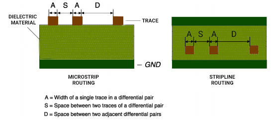
3.1.1 Traces separation: The center-to-center separation between the two traces should be at least 3 times their trace width. Without disturbing the separation between two traces, reducing the distance between the trace and the ground plane up to 10 mils helps in mitigating the crosstalk.
A high-frequency transmission medium makes it difficult for the receiver to interpret the correct information. The following transmission losses occur due to transmission media:
Googlespeedtest
Impedance mismatch can be controlled by implementing adequate termination schemes. The selection of the termination scheme depends upon the application. Let us discuss some of them.
Designing high-speed PCBs is crucial to support real-world applications. Signal transmission problems are prominent when a PCB deals with high-speed signals. An excellent high-speed board integrates various components and routing while avoiding signal integrity issues. The three main challenges we face in high-frequency boards are signal integrity, EMI/EMC, and dielectric loss.
PCBs also affect the EMI/EMC performance of the system. Auto-routed boards generally abide by the design rules (DRC) and do not meet the electromagnetic compatibility requirements.
WiFispeedtest
For expert insights into high-speed and HDI designs, see high-speed and HDI PCB design strategies by Syed Ubaid Ali Warsi
Signal integrity: Ideally, in a PCB, a signal should travel from a source (Tx) to a load (Rx) unimpaired/ unadulterated. But practically, it does not happen. The signal reaches the load with some losses (impedance mismatch, crosstalk, attenuation, reflection, and switching issues). Signal integrity (SI) is the term defined to measure these signal distortions in the high-frequency regime. Signal integrity helps to predict and understand these critical issues by providing practical solutions.
Crosstalk can be prevented by separating the traces, placing ground planes between the layers, and using low-dielectric material.
This current exits the device through the internal ground through pins that have impedance onto the ground. The switching current develops a voltage in this impedance. Thus, there is a voltage difference between the device and the board ground.
TMspeedtest
1.1.6 Differential pair termination: It requires a termination resistor between the signals at the receiving device. The termination resistor must match the differential load impedance (typically 100Ω).
In this blog post, we will be discussing the following factors that require attention while dealing with high-speed signals in a PCB design
To learn about highly reliable materials that can be used in your high-speed applications, see OhmegaPly and TCR Materials with Embedded Passives Technology in PCB Manufacturing
3.1.2 Placement of solid ground planes: Crosstalk between different layers can be prevented by placing solid ground planes between them. Though adding planes increases cost, they resolve SI problems like controlling trace impedance, reducing bypass capacitor current loop, and power supply impedance, etc.
Fastspeedtest
Aug 9, 2023 — Wincon Security's expertise in loss prevention serves as a beacon of hope for retailers seeking to secure their premises and assets.
Using the εr value, designers can evaluate the velocity (Vp) at which the signal flows and propagation delay (tPD). These parameters help to determine the length at which the trace should be considered a transmission line. The graph below depicts how insertion loss increases with signal frequency. The insertion loss (per inch) is measured for FR-4 (glass epoxy) and high-frequency Rogers RO4350B material. Higher insertion loss may lead to more attenuation. Click here for more insight on PCB materials and laminates.
by L Kleygrewe · 2024 · Cited by 36 — VR SBT can elicit perceived stress, mental effort, and average HR that resemble or exceed responses in RL SBT, providing a promising tool to complement police ...

At low frequencies (>1kHz), the signals remain within the data characterization limits, and the system performs as intended. When speed increases, the higher frequency impact comes into play, resulting in ringing, crosstalk, reflections, ground bounce, and impedance mismatch issues. It affects not only the digital properties of the system but the analog properties as well. These issues are more prone to increasing data rates for I/O and memory interfaces. Practically, these issues can be avoided by employing advanced PCB design services or by following strict layout guidelines. The signal routing, termination schemes, and power distribution techniques can help the designers to realize an effective PCB.
Being electronic industry enthusiasts, we all know when current, say signal, travels through a wire it generates magnetic fields around its vicinity. If two wires are nearby, then there is the possibility that the two magnetic fields will interact, causing energy cross-coupling between two signals called crosstalk.
Skin effect: High-frequency signals are also responsible for generating waveforms with varying current values. Such signals have their self-inductance values, which initiate an increased inductive reactance at high frequencies. It is responsible for the reduction in the conductive area on the PCB surface, more resistance, and attenuation in the signal strength. The skin-effect can be reduced by increasing the track width but it is not feasible always.
Speedtest
Signals with frequencies ranging from 50 MHz to as high as 3 GHz are considered high-speed signals, such as clock signals. Ideally, a clock signal is a square wave, but it is practically impossible to change its ‘LOW’ level to ‘HIGH’ level (and vice versa) instantly. It has a specific rise and fall time, due to which it appears to be a trapezoid in the time domain. It is worth noticing that the amplitude of the higher frequency harmonics of the clock signal in the frequency domain depends upon its rise and fall time. If the rise time is longer, then the magnitude of the harmonics will become smaller.
To understand the role of return paths in maintaining SI in connectors, see how to assemble connectors and cables for signal integrity.
Note: The maximum crosstalk value is the difference between the expected voltage at the receiver and the receiver threshold.
Virtual Reality has become an increasingly valuable tool in learning and development, allowing your education to extend beyond an eLearning course or ...
While driving on a remote highway, indecisive architect Vincent Eastman is torn between reuniting with his estranged frigid calculating wife Sally or taking up with his lover Olivia Marshak,... Read allWhile driving on a remote highway, indecisive architect Vincent Eastman is torn between reuniting with his estranged frigid calculating wife Sally or taking up with his lover Olivia Marshak, a magazine writer.While driving on a remote highway, indecisive architect Vincent Eastman is torn between reuniting with his estranged frigid calculating wife Sally or taking up with his lover Olivia Marshak, a magazine writer.
Internetspeedtest
Skydio AI-powered autonomous drones for public safety drone as first responder (DFR) programs, critical infrastructure inspection, site security, defense,
In high-speed designs, signal integrity and EMC understanding and implementation during design play an important role. Signal integrity is all about identifying and eliminating factors responsible for degrading a signal’s quality when it travels through a medium from one point to another on a PCB.
1.1.2 Thevenin termination scheme: It is an alternative to the parallel termination scheme, where the terminating resistor (RT) is split into two separate resistors, which is equal to the line impedance (when combined). This scheme reduces the total current draw from the source and adds current drawn from the power supply because the resistors are placed between VCC and ground.
That’s why it’s always advised to ensure that components are properly placed and traces are optimally routed. It helps to realize products that fulfill all electromagnetic compatibility and signal integrity requirements on time within the given budget. Designing an electromagnetic-compatible PCB can improve the overall system’s performance. Learn more about PCB design guidelines for EMI and EMC.
Oct 30, 2024 — Decisions in high-stakes scenarios require the judgment and experience that only human officers can provide, but can be enriched with AI.
The velocity of the signal traveling through the PCB depends upon the dielectric constant of the PCB. Let’s have an example: when frequency surpasses 5 GHz, the dielectric constant of FR-4 (4.7) drops to 4.
Vincent Eastman: [while on payphone] ... I'm crazy about you. I've always been crazy about you. I'm always gonna be crazy about you. Oh by the way, this is Vincent. Vincent Eastman.
Oil Absorbent Action Mats are designed to soak up contaminants such as hydraulic fluids, coolants, water, condensation, oils and solvents to help prevent ...
speedtest测速
1.1.3 Active parallel termination: Here, the terminating resistor equal to the line impedance (Z0) is placed in the path of bias voltage. The bias voltage is arranged so that the output drivers can extract current from both high and low-level signals. This technique requires a separate voltage source that can sink and source currents to match the output transfer rates.
Signal integrity becomes critical when a PCB operates at high frequency since signal rise times are low. Adopting adequate termination schemes, attenuation control, crosstalk, and ground bounce prevention can help the designers realize a PCB that can work seamlessly at high frequency. Additionally, an EMI-compliant design is also essential. In the comments section, let us know if you require assistance designing an efficient high-speed PCB.
This voltage difference is known as ground bounce. The ground bounce causes a ‘LOW’ output to be seen as ‘HIGH’ by other devices on the board. Ground bounce can be reduced by adopting solutions like:
The most commonly used laminate material is FR-4. It is very cost-effective as long as the board frequencies kept in the range from 2.5 to 3 GHz. At high speed, materials like Rogers RO4350 have better properties than the FR-4. The only trade-off is cost. Non-FR-4 materials are expensive.
3.1.3 Low dielectric constant material: Material with low dielectric constant overcomes crosstalk by reducing the mutual capacitance/stray capacitance between traces.
This parameter is important for faster and longer trace runs. The three factors that affect impedance control are substrate material, trace width, and height of the trace from the ground/power plane.


 Ms.Cici
 8618319014500